- 您現(xiàn)在的位置:買(mǎi)賣(mài)IC網(wǎng) > PDF目錄361031 > LM611MN (NATIONAL SEMICONDUCTOR CORP) Operational Amplifier and Adjustable Reference PDF資料下載
參數(shù)資料
| 型號(hào): | LM611MN |
| 廠商: | NATIONAL SEMICONDUCTOR CORP |
| 元件分類(lèi): | 運(yùn)動(dòng)控制電子 |
| 英文描述: | Operational Amplifier and Adjustable Reference |
| 中文描述: | OP-AMP, 7000 uV OFFSET-MAX, 0.5 MHz BAND WIDTH, PDIP8 |
| 封裝: | PLASTIC, DIP-8 |
| 文件頁(yè)數(shù): | 12/17頁(yè) |
| 文件大小: | 735K |
| 代理商: | LM611MN |
第1頁(yè)第2頁(yè)第3頁(yè)第4頁(yè)第5頁(yè)第6頁(yè)第7頁(yè)第8頁(yè)第9頁(yè)第10頁(yè)第11頁(yè)當(dāng)前第12頁(yè)第13頁(yè)第14頁(yè)第15頁(yè)第16頁(yè)第17頁(yè)
Application Information
(Continued)
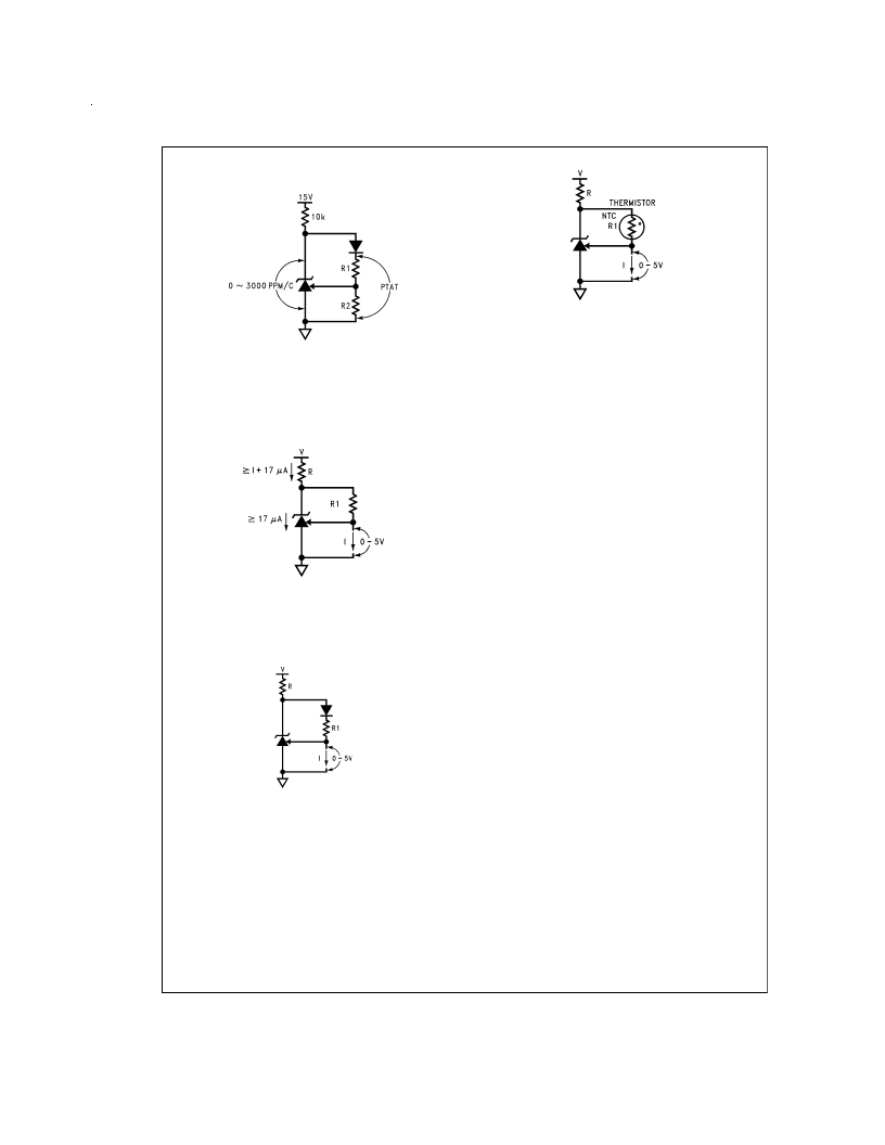
Connecting a resistor across Cathode-to-FEEDBACK cre-
ates a 0 TC current source, but a range of TCs may be syn-
thesized.
I = Vr/R1 = 1.24/R1
Hysteresis
The reference voltage depends, slightly, on the thermal his-
tory
of
the
die.
Competitive
vary— always check the data sheet for any given device. Do
not assume that no specification means no hysteresis.
micro-power
products
OPERATIONAL AMPLIFIER
The amp or the reference may be biased in any way with no
effect on the other, except when a substrate diode conducts
(see Guaranteed Electrical Characteristics Note 1). The amp
may have inputs outside the common-mode range, may be
operated as a comparator, or have all terminals floating with
no effect on the reference (tying inverting input to output and
non-inverting input to V
on unused amp is preferred).
Choosing operating points that cause oscillation, such as
driving too large a capacitive load, is best avoided.
Op Amp Output Stage
The op amp, like the LM124 series, has a flexible and rela-
tively wide-swing output stage. There are simple rules to op-
timize output swing, reduce cross-over distortion, and opti-
mize capacitive drive capability:
1.
Output Swing: Unloaded, the 42 μA pull-down will bring
the output within 300 mV of V
over the military tempera-
ture range. If more than 42 μAis required, a resistor from
output to V
will help. Swing across any load may be im-
proved slightly if the load can be tied to V
+
, at the cost of
poorer sinking open-loop voltage gain.
2.
Cross-over Distortion: The LM611 has lower cross-over
distortion (a 1 V
deadband versus 3 V
for the
LM124), and increased slew rate as shown in the char-
acteristic curves.Aresistor pull-up or pull-down will force
class-A operation with only the PNP or NPN output tran-
sistor conducting, eliminating cross-over distortion.
3.
Capacitive Drive: Limited by the output pole caused by
the
output
resistance
driving
pull-down resistor conducting 1 mA or more reduces the
output stage NPN r
e
until the output resistance is that of
the current limit 25
. 200 pF may then be driven without
oscillation.
capacitive
loads,
a
Op Amp Input Stage
The lateral PNP input transistors, unlike those of most op
amps, have BV
equal to the absolute maximum supply
voltage. Also, they have no diode clamps to the positive sup-
ply nor across the inputs. These features make the inputs
look like high impedances to input sources producing large
differential and common-mode voltages.
DS009221-21
FIGURE 8. Diode in Series with R1 Causes
Voltage Across R1 and R2 to be Proportional
to Absolute Temperature (PTAT)
DS009221-22
FIGURE 9. Current Source is Programmed by R1
DS009221-23
FIGURE 10. Proportional-to-Absolute-
Temperature Current Source
DS009221-24
FIGURE 11. Negative TC Current Source
www.national.com
12
相關(guān)PDF資料 |
PDF描述 |
|---|---|
| LM612IM | Dual-Channel Comparator and Reference |
| LM612IN | Dual-Channel Comparator and Reference |
| LM612 | Dual-Channel Comparator and Reference |
| LM612AIN | Dual-Channel Comparator and Reference |
| LM612AMN | Dual-Channel Comparator and Reference |
相關(guān)代理商/技術(shù)參數(shù) |
參數(shù)描述 |
|---|---|
| LM612 | 制造商:NSC 制造商全稱(chēng):National Semiconductor 功能描述:Dual-Channel Comparator and Reference |
| LM6121 | 制造商:NSC 制造商全稱(chēng):National Semiconductor 功能描述:High Speed Buffer |
| LM6121_04 | 制造商:NSC 制造商全稱(chēng):National Semiconductor 功能描述:High Speed Buffer |
| LM6121H | 制造商:Texas Instruments 功能描述: |
| LM6121H/883 | 制造商:NSC 制造商全稱(chēng):National Semiconductor 功能描述:High Speed Buffer |
發(fā)布緊急采購(gòu),3分鐘左右您將得到回復(fù)。