- 您現在的位置:買賣IC網 > PDF目錄361035 > LM9061 (National Semiconductor Corporation) Power MOSFET Driver with Lossless Protection PDF資料下載
參數資料
| 型號: | LM9061 |
| 廠商: | National Semiconductor Corporation |
| 英文描述: | Power MOSFET Driver with Lossless Protection |
| 中文描述: | 功率MOSFET驅動器,帶有無損保護 |
| 文件頁數: | 7/14頁 |
| 文件大小: | 234K |
| 代理商: | LM9061 |
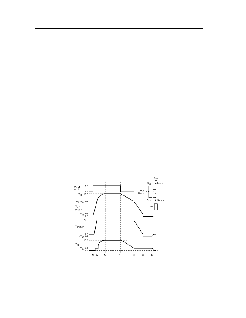
Application Hints
(Continued)
TURN ON AND TURN OFF CHARACTERISTICS
The actual rate of change of the voltage applied to the gate
of the power device is directly dependent on the input ca-
pacitances of the MOSFET used. These times are important
to know if the power to the load is to be applied repetitively
as is the case with pulse width modulation drive. Of concern
are the capacitances from gate to drain, C
GD
, and from gate
to source, C
GS
. Figure 2 details the turn ON and turn OFF
intervals in a typical application. An inductive load is as-
sumed to illustrate the output transient voltage to be expect-
ed. At time t1, the ON/OFF input goes high. The output,
which drives the gate of the MOSFET, immediately pulls the
gate voltage towards the V
CC
supply of the LM9061. The
source current from pin 4 is typically 30 mA which quickly
charges C
GD
and C
GS
. As soon as the gate reaches the
V
GS(ON)
threshold of the MOSFET, the switch turns ON and
the source voltage starts rising towards V
CC
. V
GS
remains
equal to the threshold voltage until the source reaches V
CC
.
While V
GS
is constant only C
GD
is charging. When the
source voltage reaches V
CC
, at time t2, the charge pump
takes over the drive of the gate to ensure that the MOSFET
remains ON.
The charge pump is basically a small internal capacitor that
acquires and transfers charge to the output pin. The clock
rate is set internally at typically 300 kHz. In effect the charge
pump acts as a switched capacitor resistor (approximately
67k) connected to a voltage that is clamped at 13V above
the Sense input pin of the LM9061 which is equal to the V
CC
supply in typical applications. The gate voltage rises above
V
CC
in an exponential fashion with a time constant depen-
dent upon the sum of C
GD
and C
GS
. At this time however
the load is fully energized. At time t3, the charge pump
reaches its maximum potential and the switch remains ON.
At time t4, the ON/OFF input goes low to turn OFF the
MOSFET and remove power from the load. At this time the
charge pump is disconnected and an internal 110
m
A cur-
rent sink begins to discharge the gate input capacitances to
ground. The discharge rate (
D
V/
D
T) is equal to 110
m
A/
(C
GD
a
C
GS
).
The load is still fully energized until time t5 when the gate
voltage has reached a potential of the source voltage (V
CC
)
plus the V
GS(ON)
threshold voltage of the MOSFET. Be-
tween time t5 and t6, the V
GS
voltage remains constant and
the source voltage follows the gate voltage. With the volt-
age on C
GD
held constant the discharge rate now becomes
110
m
A/C
GD
.
At time t6 the source voltage reaches 0V. As the gate
moves below the V
GS(ON)
threshold the MOSFET tries to
turn OFF. With an inductive load, if the current in the load
has not collapsed to zero by time t6, the action of the
MOSFET turning OFF will create a negative voltage tran-
sient (flyback) across the load. The negative transient will
be clamped to
b
V
GS(ON)
because the MOSFET must turn
itself back ON to continue conducting the load current until
the energy in the inductance has been dissipated (at time
t7).
MOSFET PROTECTION CIRCUITRY
A unique feature of the LM9061 is the ability to sense ex-
cessive power dissipation in the MOSFET and latch it OFF
to prevent permanent failure. Instead of sensing the actual
current flowing through the MOSFET to the load, which typi-
cally requires a small valued power resistor in series with
the load, the LM9061 monitors the voltage drop from drain
to source, V
DS
, across the MOSFET. This ‘‘lossless’’ tech-
nique allows all of the energy available from the supply to be
conducted to the load as required. The only power loss is
that of the MOSFET itself and proper selection of a particu-
lar power device for an application will minimize this con-
cern. Another benefit of this technique is that all applica-
tions use only standard inexpensive
(/4
W or less resistors.
To utilize this lossless protection technique requires knowl-
edge of key characteristics of the power MOSFET used. In
any application the emphasis for protection can be placed
on either the power MOSFET or on the amount of current
delivered to the load, with the assumption that the selected
MOSFET can safely handle the maximum load current.
TL/H/12317–9
FIGURE 2. Turn ON and Turn OFF Waveforms
7
相關PDF資料 |
PDF描述 |
|---|---|
| LM9061N | Power MOSFET Driver with Lossless Protection |
| LM9070 | Low-Dropout System Voltage Regulator with Keep-Alive ON/OFF Control |
| LM9070M | Low-Dropout System Voltage Regulator with Keep-Alive ON/OFF Control |
| LM9070S | Low-Dropout System Voltage Regulator with Keep-Alive ON/OFF Control |
| LM9070T | Low-Dropout System Voltage Regulator with Keep-Alive ON/OFF Control |
相關代理商/技術參數 |
參數描述 |
|---|---|
| LM9061EVM | 功能描述:EVAL BOARD FOR LM9061 制造商:texas instruments 系列:- 零件狀態:在售 主要用途:電源管理,高壓側驅動器(外部 FET) 嵌入式:- 使用的 IC/零件:LM9061 主要屬性:- 輔助屬性:- 所含物品:板 標準包裝:1 |
| LM9061M | 功能描述:功率驅動器IC RoHS:否 制造商:Micrel 產品:MOSFET Gate Drivers 類型:Low Cost High or Low Side MOSFET Driver 上升時間: 下降時間: 電源電壓-最大:30 V 電源電壓-最小:2.75 V 電源電流: 最大功率耗散: 最大工作溫度:+ 85 C 安裝風格:SMD/SMT 封裝 / 箱體:SOIC-8 封裝:Tube |
| LM9061M/NOPB | 功能描述:功率驅動器IC High-Side Pwr Mosfet Driver RoHS:否 制造商:Micrel 產品:MOSFET Gate Drivers 類型:Low Cost High or Low Side MOSFET Driver 上升時間: 下降時間: 電源電壓-最大:30 V 電源電壓-最小:2.75 V 電源電流: 最大功率耗散: 最大工作溫度:+ 85 C 安裝風格:SMD/SMT 封裝 / 箱體:SOIC-8 封裝:Tube |
| LM9061M/NOPB | 制造商:Texas Instruments 功能描述:IC, MOSFET DRIVER, SOIC-8 |
| LM9061MX | 功能描述:功率驅動器IC RoHS:否 制造商:Micrel 產品:MOSFET Gate Drivers 類型:Low Cost High or Low Side MOSFET Driver 上升時間: 下降時間: 電源電壓-最大:30 V 電源電壓-最小:2.75 V 電源電流: 最大功率耗散: 最大工作溫度:+ 85 C 安裝風格:SMD/SMT 封裝 / 箱體:SOIC-8 封裝:Tube |
發布緊急采購,3分鐘左右您將得到回復。