- 您現在的位置:買賣IC網 > PDF目錄361035 > LM9831 (National Semiconductor Corporation) LM9831 42-Bit Color, 1200dpi USB Image Scanner PDF資料下載
參數資料
| 型號: | LM9831 |
| 廠商: | National Semiconductor Corporation |
| 英文描述: | LM9831 42-Bit Color, 1200dpi USB Image Scanner |
| 中文描述: | LM9831 42位彩色,1200dpi的USB圖像掃描儀 |
| 文件頁數: | 5/41頁 |
| 文件大小: | 320K |
| 代理商: | LM9831 |
第1頁第2頁第3頁第4頁當前第5頁第6頁第7頁第8頁第9頁第10頁第11頁第12頁第13頁第14頁第15頁第16頁第17頁第18頁第19頁第20頁第21頁第22頁第23頁第24頁第25頁第26頁第27頁第28頁第29頁第30頁第31頁第32頁第33頁第34頁第35頁第36頁第37頁第38頁第39頁第40頁第41頁
5
www.national.com
Note 1:
Absolute Maximum Ratings indicate limits beyond which damage to the device may occur. Operating Ratings indicate conditions for which the device is functional,
but do not guarantee specific performance limits. For guaranteed specifications and test conditions, see the Electrical Characteristics. The guaranteed specifications apply
only for the test conditions listed. Some performance characteristics may degrade when the device is not operated under the listed test conditions.
Note 2:
All voltages are measured with respect to GND=AGND=DGND=0V, unless otherwise specified.
Note 3:
When the input voltage (V
IN
) at any pin exceeds the power supplies (V
IN
<GND or V
IN
>V
A
or V
D
), the current at that pin should be limited to 25mA. The 50mA
maximum package input current rating limits the number of pins that can simultaneously safely exceed the power supplies with an input current of 25mA to two.
Note 4:
The maximum power dissipation must be derated at elevated temperatures and is dictated by T
J
max,
Θ
JA
and the ambient temperature, T
A
. The maximum allow-
able power dissipation at any temperature is P
D
= (T
J
max - T
A
) /
Θ
JA
. T
J
max = 150°C for this device. The typical thermal resistance (
Θ
JA
) of this part when board mounted
is 53°C/W
Note 5:
Human body model, 100pF capacitor discharged through a 1.5k
resistor. Machine model, 200pF capacitor discharged through a 0
resistor.
Note 6:
See AN-450 “Surface Mounting Methods and Their Effect on Product Reliability” or the section titled “Surface Mount” found in any National Semiconductor Linear
Data Book for other methods of soldering surface mount devices.
Note 7:
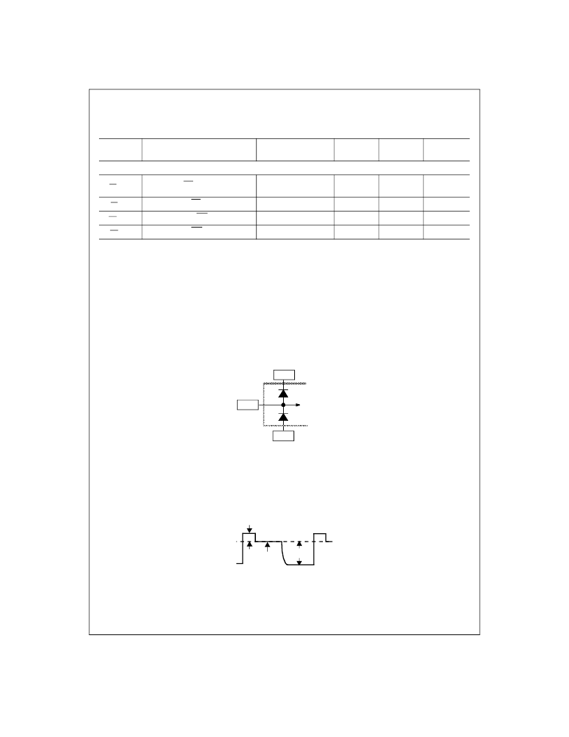
Two diodes clamp the OS analog inputs to
AGND
and
VA
as shown below. This input protection, in combination with the external clamp capacitor and the output
impedance of the sensor, prevents damage to the LM9831 from transients during power-up.
Note 8:
For best performance, it is required that all supply pins be powered from the same power supply with separate bypass capacitors at each supply pin.
Note 9:
Typicals are at T
J
=T
A
=25°C, f
CRYSTAL IN
= 48MHz, and represent most likely parametric norm.
Note 10:
Tested limits are guaranteed to National's AOQL (Average Outgoing Quality Level).
Note 11:
Integral linearity error is defined as the deviation of the analog value, expressed in LSBs, from the straight line that best fits the actual transfer function of the ADC.
Note 12:
V
REF
is defined as the CCD OS voltage for the reference period following the reset feedthrough pulse. V
WHITE
is defined as the peak CCD pixel output voltage for
a white (full scale) image with respect to the reference level, V
.
V
is defined as the peak positive deviation above V
of the reset feedthrough pulse. The maximum
correctable range of pixel-to-pixel V
variation is defined as the maximum variation in V
WHITE
(due to PRNU, light source intensity variation, optics, etc.) that the
LM9831 can correct for using its internal PGA.
Note 13:
PGA Gain Error is the maximum difference between the measured gain for any PGA code and the ideal gain calculated by using the formula
V
V
31
where
.
AC Electrical Characteristics
The following specifications apply for AGND=DGND=0V, V
A
=V
D
=V
DRAM
=+5.0V
DC
unless otherwise noted,
f
CRYSTAL IN
= 48MHz, MCLK DIVIDER = 1.0 (unless otherwise noted), f
MCLK
= f
CRYSTAL IN
/MCLK DIVIDER, f
ADC CLK
= f
MCLK
/8,
C
L
(databus loading) = 20pF/pin.
Boldface limits apply for T
A
=T
J
=T
MIN
to T
MAX
; all other limits T
A
=T
J
=25°C. (Notes 8, 9, & 10)
Symbol
Parameter
Conditions
Typical
(Note 9)
Limits
(Note 10)
Units
(Limits)
DRAM Timing (Figure 1)
t
RD SETUP
Data valid to RD rising edge
V
DRAM
=5.0V
V
DRAM
=3.3V
26
35
ns (min)
ns (min)
t
RD HOLD
Data valid after RD rising edge
0
ns (min)
t
WR SETUP
Data valid before WR falling edge
5
ns (min)
t
WR HOLD
Data valid after WR rising edge
10
ns (min)
OS Input
AGND
VA
To Internal
Circuitry
V
WHITE
V
REF
V
RFT
CCD Output Signal
GainPGA
---
G0
X--------------------------
+
=
X
G31
G0
–
(
)
32
-----
=
相關PDF資料 |
PDF描述 |
|---|---|
| LM9831CCVJDX | LM9831 42-Bit Color, 1200dpi USB Image Scanner |
| LM9832CCVJD | LM9832 42-Bit Color, 1200dpi USB Image Scanner |
| LM9832 | LM9832 42-Bit Color, 1200dpi USB Image Scanner |
| LM9833CCVJD | LM9833 48-Bit Color, 1200dpi USB Image Scanner |
| LM9833 | LM9833 48-Bit Color, 1200dpi USB Image Scanner |
相關代理商/技術參數 |
參數描述 |
|---|---|
| LM9831CCVJD | 制造商:NSC 制造商全稱:National Semiconductor 功能描述:LM9831 42-Bit Color, 1200dpi USB Image Scanner |
| LM9831CCVJDX | 制造商:NSC 制造商全稱:National Semiconductor 功能描述:LM9831 42-Bit Color, 1200dpi USB Image Scanner |
| LM9832 | 制造商:NSC 制造商全稱:National Semiconductor 功能描述:LM9832 42-Bit Color, 1200dpi USB Image Scanner |
| LM9832B-B WAF | 制造商:Texas Instruments 功能描述: |
| LM9832B-E WAF | 制造商:Texas Instruments 功能描述: |
發布緊急采購,3分鐘左右您將得到回復。