- 您現在的位置:買賣IC網 > PDF目錄361035 > LM9832CCVJD (NATIONAL SEMICONDUCTOR CORP) LM9832 42-Bit Color, 1200dpi USB Image Scanner PDF資料下載
參數資料
| 型號: | LM9832CCVJD |
| 廠商: | NATIONAL SEMICONDUCTOR CORP |
| 元件分類: | 消費家電 |
| 英文描述: | LM9832 42-Bit Color, 1200dpi USB Image Scanner |
| 中文描述: | SPECIALTY CONSUMER CIRCUIT, PQFP100 |
| 封裝: | PLASTIC, TQFP-100 |
| 文件頁數: | 7/42頁 |
| 文件大小: | 337K |
| 代理商: | LM9832CCVJD |
第1頁第2頁第3頁第4頁第5頁第6頁當前第7頁第8頁第9頁第10頁第11頁第12頁第13頁第14頁第15頁第16頁第17頁第18頁第19頁第20頁第21頁第22頁第23頁第24頁第25頁第26頁第27頁第28頁第29頁第30頁第31頁第32頁第33頁第34頁第35頁第36頁第37頁第38頁第39頁第40頁第41頁第42頁
7
www.national.com
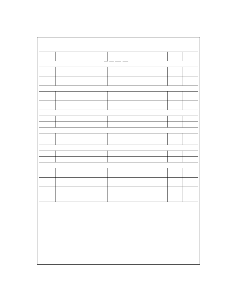
Digital Output Characteristics for D0-D15, A0-A9, RD, WR, RAS, CAS (DRAM Interface)
V
OUT(1)
Logical “1” Output Voltage
V
DRAM
=4.75V, I
OUT
=-4mA
V
DRAM
=2.85V, I
OUT
=-4mA
2.4
2.4
V (min)
V (min)
V
OUT(0)
Logical “0” Output Voltage
V
DRAM
=4.75V, I
OUT
=4mA
V
DRAM
=2.85V, I
OUT
=4mA
0.4
0.4
V (max)
V (max)
Digital Output Characteristics for A, B, A, B
V
OUT(1)
Logical “1” Output Voltage
V
DRAM
=4.75V, I
OUT
=-10mA
V
DRAM
=2.85V, I
OUT
=-10mA
2.4
2.4
V (min)
V (min)
V
OUT(0)
Logical “0” Output Voltage
V
DRAM
=4.75V, I
OUT
=4mA
V
DRAM
=2.85V, I
OUT
=4mA
0.4
0.4
V (max)
V (max)
Digital Output Characteristics for MISC I/O 1-6, TR1, TR2, 1, 2, RS, CP1, CP2, LAMP
R
, LAMP
G
, LAMP
B
V
OUT(1)
Logical “1” Output Voltage
V
D
=4.75V, I
OUT
=-4mA
2.4
V (min)
V
OUT(0)
Logical “0” Output Voltage
V
D
=4.75V, I
OUT
=4mA
0.4
V (max)
Digital Output Characteristics for D+, D-
V
OUT(1)
Logical “1” Output Voltage
V
D
=4.75V, I
OUT
=-1mA
2.4
V (min)
V
OUT(0)
Logical “0” Output Voltage
V
D
=4.75V, I
OUT
=3mA
0.4
V (max)
CRYSTAL IN, CRYSTAL OUT Characteristics
XTAL
OUT DC
CRYSTAL OUT Bias Level (Offset)
0.8
V
XTAL
OUT AC
CRYSTAL OUT Amplitude
f
CRYSTAL
= 48MHz
0.8
V
P-P
Power Supply Characteristics (Note 14)
I
A
Analog Supply Current
(V
A
pins)
Operating (Bias Current = 80%)
65
91
mA (max)
I
D
Digital Supply Current
(V
D
pins)
Operating (Bias Current = 80%)
35
41
mA (max)
I
DRAM
DRAM Supply Current
(V
DRAM
pins)
Operating, V
DRAM
= 5V
Operating, V
DRAM
= 3V
2
1
8
5
mA (max)
mA (max)
I
SUSPEND
Total Suspend Current (I
A
+I
D
+I
DRAM
)
19
175
μA (max)
DC and Logic Electrical Characteristics
(Continued)
The following specifications apply for AGND=DGND=0V, V
A
=V
D
=V
DRAM
=+5.0V
DC
unless otherwise noted,
f
CRYSTAL IN
= 48MHz.
Boldface limits apply for T
A
=T
J
=T
MIN
to T
MAX
; all other limits T
A
=T
J
=25°C. (Notes 8, 9, & 10)
Symbol
Parameter
Conditions
Typical
(Note 9)
Limits
(Note 10)
Units
(Limits)
L
相關PDF資料 |
PDF描述 |
|---|---|
| LM9832 | LM9832 42-Bit Color, 1200dpi USB Image Scanner |
| LM9833CCVJD | LM9833 48-Bit Color, 1200dpi USB Image Scanner |
| LM9833 | LM9833 48-Bit Color, 1200dpi USB Image Scanner |
| LM98501CCVBH | 10-Bit, 27 MSPS Camera Signal Processor |
| LM98501 | 10-Bit, 27 MSPS Camera Signal Processor |
相關代理商/技術參數 |
參數描述 |
|---|---|
| LM9832CCVS-B | 制造商:Texas Instruments 功能描述: |
| LM9833 | 制造商:NSC 制造商全稱:National Semiconductor 功能描述:LM9833 48-Bit Color, 1200dpi USB Image Scanner |
| LM9833B-F WAF | 制造商:Texas Instruments 功能描述: |
| LM9833CCVJD | 制造商:Texas Instruments 功能描述:USB Image Scanner 100-Pin TQFP |
| LM9833CCVJD NOPB | 制造商:Texas Instruments 功能描述:Bulk |
發布緊急采購,3分鐘左右您將得到回復。