- 您現在的位置:買賣IC網 > PDF目錄361038 > LMC7215IMX (NATIONAL SEMICONDUCTOR CORP) Micro-Power, Rail-to-Rail CMOS Comparators with Open-Drain/Push-Pull Outputs and TinyPak⑩ Package PDF資料下載
參數資料
| 型號: | LMC7215IMX |
| 廠商: | NATIONAL SEMICONDUCTOR CORP |
| 元件分類: | 運動控制電子 |
| 英文描述: | Micro-Power, Rail-to-Rail CMOS Comparators with Open-Drain/Push-Pull Outputs and TinyPak⑩ Package |
| 中文描述: | COMPARATOR, 8000 uV OFFSET-MAX, 17000 ns RESPONSE TIME, PDSO8 |
| 封裝: | SOIC-8 |
| 文件頁數: | 6/11頁 |
| 文件大小: | 360K |
| 代理商: | LMC7215IMX |
Typical Performance Characteristics
T
A
= 25C unless otherwise specified (Continued)
Application Information
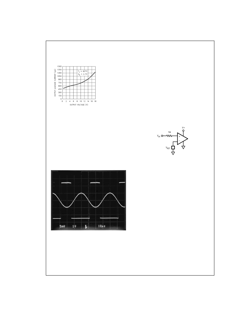
RESPONSE TIME
Depending upon the amount of overdrive, the delay will typi-
cally be between 10 μs to 200 μs. The curve showing delay
vs overdrive in the “Typical Characteristics” section shows
the delay time when the input is preset with 100 mV across
the inputs and then is driven the other way by 1 mV to 500
mV.
The transition from high to low or low to high is fast. Typically
1 μs rise and 400 ns fall.
With a small signal input, the comparators will provide a
square wave output from sine wave inputs at frequencies as
high as 25 kHz. Figure 1shows a worst case example where
a
±
5 mV sine wave is applied to the input. Note that the out-
put is delayed by almost 180.
NOISE
Most comparators have rather low gain. This allows the out-
put to spend time between high and low when the input sig-
nal changes slowly. The result is the output may oscillate be-
tween high and low when the differential input is near zero.
The exceptionally high gain of these comparators, 10,000V/
mV, eliminates this problem. Less then 1 μV of change on
the input will drive the output from one rail to the other rail.
If the input signal is noisy, the output cannot ignore the noise
unless some hysteresis is provided by positive feedback.
INPUT VOLTAGE RANGE
The LMC7215/25 have input voltage ranges that are larger
than the supply voltage guarantees that signals from other
parts of the system cannot overdrive the inputs. This allows
sensing supply current by connecting one input directly to
the V
+
line and the other to the other side of a current sense
resistor. The same is true if the sense resistor is in the
ground return line.
Sensing supply voltage is also easy by connecting one input
directly to the supply.
The inputs of these comparators are protected by diodes to
both supplies. This protects the inputs from both ESD as well
as signals that greatly exceed the supply voltages. As a re-
sult, current will flow through these forward biased diodes
whenever the input voltage is more than a few hundred mil-
livolts larger than the supplies. Until this occurs, there is es-
sentially no input current. As a result, placing a large resistor
in series with any input that may be exposed to large volt-
ages, will limit the input current but have no other noticeable
effect.
If the input current is limited to less than 5 mA by a series re-
sistor, (see Figure 2), a threshold or zero crossing detector,
that works with inputs from as low as a few millivolts to as
high as 5,000V, is made with only one resistor and the com-
parator.
INPUTS
As mentioned above, these comparators have near zero in-
put current. This allows very high resistance circuits to be
used without any concern for matching input resistances.
Output Leakage Current
vs Output Voltage
LMC7225
DS012853-20
DS012853-4
FIGURE 1.
DS012853-5
FIGURE 2.
www.national.com
6
相關PDF資料 |
PDF描述 |
|---|---|
| LMC7225IM | Micro-Power, Rail-to-Rail CMOS Comparators with Open-Drain/Push-Pull Outputs and TinyPak⑩ Package |
| LMC7225IM5 | Micro-Power, Rail-to-Rail CMOS Comparators with Open-Drain/Push-Pull Outputs and TinyPak⑩ Package |
| LMC7225IM5X | Micro-Power, Rail-to-Rail CMOS Comparators with Open-Drain/Push-Pull Outputs and TinyPak⑩ Package |
| LMC7225IMX | Micro-Power, Rail-to-Rail CMOS Comparators with Open-Drain/Push-Pull Outputs and TinyPak⑩ Package |
| LMC7221BIM | Tiny CMOS Comparator with Rail-To-Rail Input and Open Drain Output |
相關代理商/技術參數 |
參數描述 |
|---|---|
| LMC7215IMX/NOPB | 功能描述:校驗器 IC RoHS:否 制造商:STMicroelectronics 產品: 比較器類型: 通道數量: 輸出類型:Push-Pull 電源電壓-最大:5.5 V 電源電壓-最小:1.1 V 補償電壓(最大值):6 mV 電源電流(最大值):1350 nA 響應時間: 最大工作溫度:+ 125 C 安裝風格:SMD/SMT 封裝 / 箱體:SC-70-5 封裝:Reel |
| LMC7215QIM5/NOPB | 制造商:Texas Instruments 功能描述:IC COMP MICRPWR R-R CMOS SOT23-5 制造商:Texas Instruments 功能描述:LOW POWER AMPLIFIER IC |
| LMC7215QIM5NOPB | 制造商:Texas Instruments 功能描述: |
| LMC7215QIM5X/NOPB | 制造商:Texas Instruments 功能描述:IC COMP MICRPWR R-R CMOS SOT23-6 制造商:Texas Instruments 功能描述:LOW POWER AMPLIFIER IC |
| LMC7215QIM5XNOPB | 制造商:Texas Instruments 功能描述: |
發布緊急采購,3分鐘左右您將得到回復。