- 您現在的位置:買賣IC網 > PDF目錄361039 > LMC8101BP (NATIONAL SEMICONDUCTOR CORP) Rail-to-Rail Input and Output, 2.7V Op Amp in micro SMD package with Shutdown PDF資料下載
參數資料
| 型號: | LMC8101BP |
| 廠商: | NATIONAL SEMICONDUCTOR CORP |
| 元件分類: | 運算放大器 |
| 英文描述: | Rail-to-Rail Input and Output, 2.7V Op Amp in micro SMD package with Shutdown |
| 中文描述: | OP-AMP, 7000 uV OFFSET-MAX, 0.84 MHz BAND WIDTH, PBGA8 |
| 封裝: | MICRO, SMD-8 |
| 文件頁數: | 6/15頁 |
| 文件大小: | 709K |
| 代理商: | LMC8101BP |
+/5V Electrical Characteristics
(Continued)
Note 1:
Absolute Maximum Ratings indicate limits beyond which damage to the device may occur. Operating Ratings indicate conditions for which the device is in-
tended to be functional, but specific performance is not guaranteed. For guaranteed specifications and the test conditions, see the Electrical Characteristics.
Note 2:
Human body model, 1.5k
in series with 100pF.
Note 3:
Applies to both single-supply and split-supply operation. Continuous short circuit operation at elevated ambient temperature can result in exceeding the
maximum allowed junction temperature at 150C. Output currents in excess of 40mA over long term may adversely affect reliability.
Note 4:
The maximum power dissipation is a function of T
,
θ
and T
. The maximum allowable power dissipation at any ambient temperature is P
D
= (T
J(max)
T
A
)/
θ
JA
. All numbers apply for packages soldered directly onto a PC board.
Note 5:
Typical Values represent the most likely parametric norm.
Note 6:
All limits are guaranteed by testing or statistical analysis.
Note 7:
Positive current corresponds to current flowing into the device.
Note 8:
Slew rate is the slower of the rising and falling slew rates.
Note 9:
Shutdown Turn-on and Turn-off times are defined as the time required for the output to reach 90% and 10%, respectively, of its final peak to peak swing when
set for Rail to Rail output swing with a 100KHz sine wave, 2K
load, and A
V
= +10.
Note 10:
Limiting input pin current is only necessary for input voltages that exceed absolute maximum input voltage ratings.
Note 11:
Short circuit test is a momentary test. See Note 12.
Note 12:
Output short circuit duration is infinite for V
S
<
6V. Otherwise, extended period output short circuit may damage the device.
Note 13:
machine Model, 0
in series with 200pF.
Application Notes
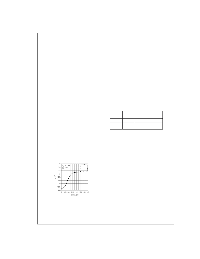
Shutdown features:
The LMC8101 is capable of being turned off in order to con-
serve power. Once in shutdown, the device supply current is
drastically reduced (1μA maximum) and the output will be
″
Tri-stated
″
.
The shutdown feature of the LMC8101 is designed for flex-
ibility. The threshold level of the SD input can be referenced
to either V
-
or V
+
by setting the level on the SL input. When
the SL input is connected to V
-
, the SD threshold level is ref-
erenced to V
-
and vice versa. This threshold will be about
1.5V from the supply tied to the SL pin. So, for this example,
the device will be in shutdown as long as the SD pin voltage
is within 1V of V
. In order to ensure that the device would not
″
chatter
″
between active and shutdown states, hysteresis is
built into the SD pin transition (see Figure 1for an illustration
of this feature). The shutdown threshold and hysteresis level
are independent of the supply voltage. Figure 1 illustration
applies equally well to the case when SL is tied to V
+
and the
horizontal axis is referenced to V
+
instead. The SD pin
should not be set within the voltage range from 1.1V to 1.9V
of the selected supply voltage since this is a transition region
and the device status will be undetermined.
Table 1 below, summarizes the status of the device when
the SL and SD pins are connected directly to V
-
or V
+
:
TABLE 1. LMC8101 Status Summary
SL
V
V
V
+
V
+
SD
V
V
+
V
+
V
LMC8101 Status
Shutdown
Active
Shutdown
Active
In case shutdown operation is not needed, as can be seen in
Table 1, the two pins SL and SD can simply be connected to
opposite supply nodes to achieve
″
Active
″
operation. The SL
and SD should always be tied to a node; if left unconnected,
these high impedance inputs will float to an undetermined
state and the device status will be undetermined as well.
With the device in shutdown, once
″
Active
″
operation is initi-
ated, there will be a finite amount of time required before the
device output is settled to its final value. This time is less
than 15μs. In addition, there may be some output spike dur-
ing this time while the device is transitioning into a fully op-
erational state. Some applications may be sensitive to this
output spike and proper precautions should be taken in order
to ensure proper operation at all times.
Tiny Package:
The LMC8101 is available in the micro SMD package as well
the 8 pin MSOP package. The micro SMD package requires
approximately 1/4 the board area of a SOT23. This package
is less than 1mm in height allowing it to be placed in absolute
minimum height clearance areas such as cellular handsets,
LCD panels, PCMCIA cards, etc. More information about the
micro
SMD
package
can
www.national.com/appinfo/microsmd.
be
found
at:
http://
DS101240-82
FIGURE 1. Supply Current vs. ’SD’ Voltage
www.national.com
6
相關PDF資料 |
PDF描述 |
|---|---|
| LMC8101BPX | Rail-to-Rail Input and Output, 2.7V Op Amp in micro SMD package with Shutdown |
| LMC8101MM | Rail-to-Rail Input and Output, 2.7V Op Amp in micro SMD package with Shutdown |
| LMC8101MMX | Rail-to-Rail Input and Output, 2.7V Op Amp in micro SMD package with Shutdown |
| LMF100 | High Performance Dual Switched Capacitor Filter |
| LMF100CCN | High Performance Dual Switched Capacitor Filter |
相關代理商/技術參數 |
參數描述 |
|---|---|
| LMC8101BP/NOPB | 制造商:Texas Instruments 功能描述:OP Amp Single GP R-R I/O |
| LMC8101BPCONV | 功能描述:BOARD EVALUATION LMC8101BP RoHS:否 類別:編程器,開發系統 >> 評估板 - 運算放大器 系列:- 產品培訓模塊:Lead (SnPb) Finish for COTS Obsolescence Mitigation Program 標準包裝:1 系列:- |
| LMC8101BPX | 制造商:Rochester Electronics LLC 功能描述: 制造商:Texas Instruments 功能描述: |
| LMC8101BPX/NOPB | 功能描述:IC OP AMP R-R I/O 8-MICROSMD RoHS:是 類別:集成電路 (IC) >> Linear - Amplifiers - Instrumentation 系列:- 標準包裝:1,000 系列:- 放大器類型:電壓反饋 電路數:4 輸出類型:滿擺幅 轉換速率:33 V/µs 增益帶寬積:20MHz -3db帶寬:30MHz 電流 - 輸入偏壓:2nA 電壓 - 輸入偏移:3000µV 電流 - 電源:2.5mA 電流 - 輸出 / 通道:30mA 電壓 - 電源,單路/雙路(±):4.5 V ~ 16.5 V,±2.25 V ~ 8.25 V 工作溫度:-40°C ~ 85°C 安裝類型:表面貼裝 封裝/外殼:14-SOIC(0.154",3.90mm 寬) 供應商設備封裝:14-SOIC 包裝:帶卷 (TR) |
| LMC8101MM | 功能描述:運算放大器 - 運放 RoHS:否 制造商:STMicroelectronics 通道數量:4 共模抑制比(最小值):63 dB 輸入補償電壓:1 mV 輸入偏流(最大值):10 pA 工作電源電壓:2.7 V to 5.5 V 安裝風格:SMD/SMT 封裝 / 箱體:QFN-16 轉換速度:0.89 V/us 關閉:No 輸出電流:55 mA 最大工作溫度:+ 125 C 封裝:Reel |
發布緊急采購,3分鐘左右您將得到回復。