- 您現(xiàn)在的位置:買賣IC網(wǎng) > PDF目錄361039 > LMF90CIN (NATIONAL SEMICONDUCTOR CORP) 4th-Order Elliptic Notch Filter PDF資料下載
參數(shù)資料
| 型號: | LMF90CIN |
| 廠商: | NATIONAL SEMICONDUCTOR CORP |
| 元件分類: | 模擬濾波器 |
| 英文描述: | 4th-Order Elliptic Notch Filter |
| 中文描述: | SWITCHED CAPACITOR FILTER, ELLIPTIC, NOTCH, PDIP14 |
| 封裝: | 0.300 INCH, PLASTIC, DIP-14 |
| 文件頁數(shù): | 12/22頁 |
| 文件大小: | 411K |
| 代理商: | LMF90CIN |
2.0 Applications Information
(Continued)
2.2 PROGRAMMING PINS
The LMF90 has five control pins that are used to program
the filter’s characteristics via a three-level logic scheme. In
dual-supply applications, these inputs are tied to either V
,
V
, or GND in order to select a particular set of characteris-
tics. For example, the W input (pin 1) sets the filter’s pass-
band width to 0.55 f
0
, 0.26 f
0
or 0.127 f
0
when the W input is
connected to V
, GND, or V
, respectively. Applying V
b
and GND to the D input (pin 10) will set the notch depth to
40 dB or 30 dB, respectively.
The R input (pin 2) is another three-level logic input, and it
sets the clock-to-center-frequency ratio to 33.33:1, 50:1, or
100:1 for input voltages equal to V
, GND, or V
, respec-
tively. Note that the clock frequency referred to here is the
frequency at the CLK pin and at the frequency divider output
(if used). This is different from the frequency at the divider’s
input. LD (pin 3) sets the frequency divider’s division factor
to either 716, 596, or 2 for input voltages equal to V
, GND,
or V
, respectively. XLS (pin 7) enables and disables the
crystal oscillator and clock divider. When XLS is connected
to the positive supply, the oscillator and divider are enabled,
and CLK is the output of the divider and can drive the clock
inputs of other LMF90s. When XLS is connected to GND,
the oscillator and divider are disabled, and the CLK pin be-
comes a clock input for CMOS-level signals. Connecting
XLS to the negative supply disables the oscillator and divid-
er and causes CLK to operate as a TTL-level clock input.
Using an external 3.579545 MHz color television crystal with
the internal oscillator and divider, it is possible to build a
power line frequency notch for 50 Hz or 60 Hz line frequen-
cies or their second and third harmonics using the LMF90. A
60 Hz notch is shown in the Typical Application circuit on
the first page of this data sheet. Connecting LD to V
a
changes the notch frequency to 50 Hz. Changing the clock-
to-center-frequency ratio to 50:1 results in a second-har-
monic notch, and a 33:1 ratio causes the LMF90 to notch
the third harmonic.
Table I illustrates 18 different combinations of filter band-
width, depth, and clock-to-center-frequency ratio obtained
by choosing the appropriate W, D, and R programming volt-
ages.
2.3 DIGITAL INPUTS AND OUTPUTS
As mentioned above, the CLK pin can serve as either an
input or an output, depending on the programming voltage
on XLS. When CLK is operating as a TTL input, it will oper-
ate properly in both dual-supply and single-supply applica-
tions, because it has two logic thresholdsDone referred to
V
, and one referred to GND. When operating as an output,
CLK swings rail-to-rail (CMOS logic levels).
XTAL1 and XTAL2 are the input and output pins for the
internal crystal oscillator. When using the internal oscillator
(XLS connected to V
), the crystal is connected between
these two pins. When the internal oscillator is not used,
XTAL2 should be left open. XTAL1 can be used as an input
for an external CMOS-level clock signal swinging from V
b
to V
. The frequency of the crystal or the external clock
applied to XTAL1 will be divided by the internal frequency
divider as determined by programming voltage on the LD
pin.
2.4 SAMPLED-DATA SYSTEM CONSIDERATIONS
OUTPUT STEPS
Because the LMF90 uses switched-capacitor techniques, its
performance differs in several ways from non-sampled (con-
tinuous) circuits. The analog signal at the input to the inter-
nal bandpass filter (pin 12) is sampled during each clock
cycle, and, since the output voltage can change only once
every clock cycle, the result is a discontinuous output signal.
The bandpass output takes the form of a series of voltage
‘‘steps’’, as shown in Figure 3. The steps are smaller when
the clock frequency is much greater than the signal frequen-
cy.
Switched-capacitor techniques are used to set the summing
amplifier’s gain. Its input and feedback ‘‘resistors’’ are actu-
ally made from switches and capacitors. Two sets of these
‘‘resistors’’ are alternated during each clock cycle. Each
time these gain-setting components are switched, there will
be no feedback connected to the op amp for a short period
of time (about 50 ns). This generates very low-amplitude
output signals at f
CLK
a
f
IN
, f
CLK
b
f
IN
, 2 f
CLK
a
f
IN
, etc.
The amplitude of each of these intermodulation compo-
nents will typically be at least 70 dB below the input signal
amplitude and well beyond the spectrum of interest.
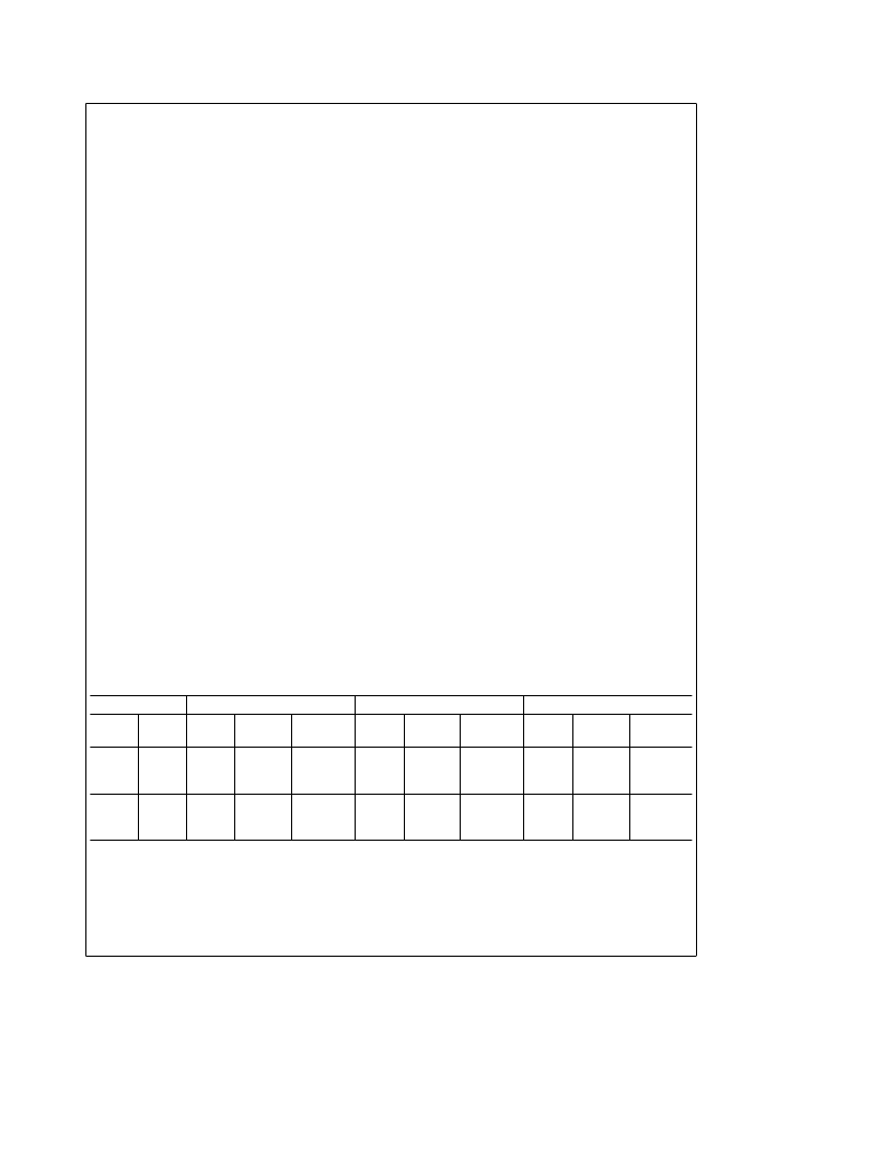
TABLE I. Operation of LMF90 Programming Pins. Values given are for nominal levels of attenuation.
V
b
(f
CLK
/f
0
e
100)
R
GND (f
CLK
/f
0
e
50)
V
a
(f
CLK
/f
0
e
33.33)
D
W
A
min
(dB)
BW/f
0
SBW/f
0
A
min
(dB)
BW/f
0
SBW/f
0
A
min
(dB)
BW/f
0
SBW/f
0
V
b
GND
V
a
V
b
GND
V
a
b
30
b
30
b
30
0.12
0.26
0.55
0.019
0.040
0.082
b
30
b
30
b
30
0.12
0.26
0.55
0.019
0.040
0.082
b
30
b
30
b
30
0.12
0.26
0.55
0.019
0.040
0.082
V
b
b
35
b
40
b
40
0.12
0.26
0.55
0.010
0.024
0.050
b
35
b
40
b
40
0.12
0.26
0.55
0.010
0.024
0.050
b
35
b
40
b
40
0.12
0.26
0.55
0.010
0.024
0.050
GND
12
相關(guān)PDF資料 |
PDF描述 |
|---|---|
| LMF90CIWM | 4th-Order Elliptic Notch Filter |
| LMF90CMJ | 4th-Order Elliptic Notch Filter |
| LMF90CCWM | 4th-Order Elliptic Notch Filter |
| LMH6550 | Differential, High Speed Op Amp |
| LMH6550MA | Differential, High Speed Op Amp |
相關(guān)代理商/技術(shù)參數(shù) |
參數(shù)描述 |
|---|---|
| LMF90CIWM | 制造商:NSC 制造商全稱:National Semiconductor 功能描述:4th-Order Elliptic Notch Filter |
| LMF90CMJ | 制造商:NSC 制造商全稱:National Semiconductor 功能描述:4th-Order Elliptic Notch Filter |
| LMF90CMJ/883 | 制造商:NSC 制造商全稱:National Semiconductor 功能描述:4th-Order Elliptic Notch Filter |
| LM-FB20F-12 | 制造商:CML Innovative Technologies 功能描述:LED SRTIP FLEXIBLE 1X26 RGB |
| LM-FB26B | 制造商:CML Innovative Technologies 功能描述:LED STRIP FLEXIBLE 1X26 BLUE |
發(fā)布緊急采購,3分鐘左右您將得到回復(fù)。