- 您現在的位置:買賣IC網 > PDF目錄361040 > LMH6624 (National Semiconductor Corporation) Single/Dual Ultra Low Noise Wideband Operational Amplifier PDF資料下載
參數資料
| 型號: | LMH6624 |
| 廠商: | National Semiconductor Corporation |
| 英文描述: | Single/Dual Ultra Low Noise Wideband Operational Amplifier |
| 中文描述: | 單/雙超寬帶低噪聲運算放大器 |
| 文件頁數: | 15/20頁 |
| 文件大小: | 985K |
| 代理商: | LMH6624 |
Application Section
(Continued)
(1)
R
f
||R
g
= R
seq
for bias current cancellation.
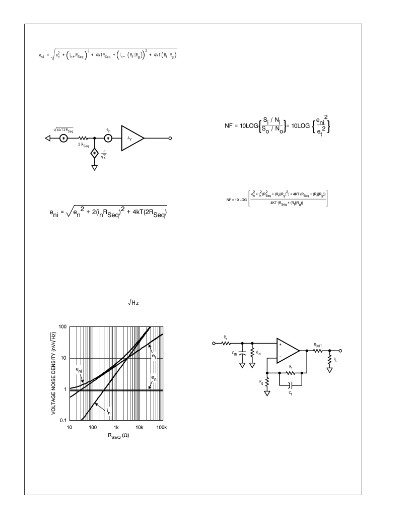
Figure 4
illus-
trates the equivalent noise model using this assumption.
Figure 5
is a plot of e
ni
against equivalent source resistance
(R
seq
) with all of the contributing voltage noise source of
Equation 2. This plot gives the expected e
for a given (R
)
which assumes R
||R
= R
for bias current cancellation.
The total equivalent output voltage noise (e
no
) is e
ni
*
A
V
.
(2)
As seen in
Figure 5
, e
ni
is dominated by the intrinsic voltage
noise (e
n
) of the amplifier for equivalent source resistances
below 33.5
. Between 33.5
and 6.43k
, e
is dominated
by the thermal noise (e
t
=
√
(4kT(2R
)) of the external
resistor. Above 6.43k
, e
ni
is dominated by the amplifier’s
current noise (i
=
√
(2) i
R
). When R
= 464
(ie.,
e
/
√
(2) i
) the contribution from voltage noise and current
noise of LMH6624/LMH6626 is equal.. For example, config-
ured with a gain of +20V/V giving a 3dB of 90MHz and
driven from R
= 25
, the LMH6624 produces a total
equivalent input noise voltage (e
ni
x
16.5μV
rms
.
1.57
*
90MHz) of
If bias current cancellation is not a requirement, then R
||R
g
need not equal R
seq
. In this case, according to Equation 1,
R
||R
should be as low as possible to minimize noise.
Results similar to Equation 1 are obtained for the inverting
configuration of
Figure 2
if R
is replaced by R
and R
is
replaced by R
+ R
. With these substitutions, Equation 1 will
yield an e
referred to the non-inverting input. Referring e
ni
to the inverting input is easily accomplished by multiplying
e
ni
by the ratio of non-inverting to inverting gains.
NOISE FIGURE
Noise Figure (NF) is a measure of the noise degradation
caused by an amplifier.
(3)
The Noise Figure formula is shown in Equation 3. The addi-
tion of a terminating resistor R
, reduces the external ther-
mal noise but increases the resulting NF. The NF is in-
creased because R
reduces the input signal amplitude thus
reducing the input SNR.
(4)
The noise figure is related to the equivalent source resis-
tance (R
) and the parallel combination of R
f
and R
g
. To
minimize noise figure.
Minimize R
f
||R
g
Choose the Optimum R
S
(R
OPT
)
R
OPT
is the point at which the NF curve reaches a minimum
and is approximated by:
R
OPT
≈
e
n
/i
n
NON-INVERTING GAINS LESS THAN 10V/V
Using the LMH6624/LMH6626 at lower non-inverting gains
requires external compensation such as the shunt compen-
sation as shown in
Figure 6
. The compensation capacitors
are chosen to reduce frequency response peaking to less
than 1dB.
INVERTING GAINS LESS THAN 10V/V
The lag compensation of
Figure 7
will achieve stability for
lower gains. It is best used for the inverting configuration
because of its affect on the non-inverting input impedance.
20058921
FIGURE 4. Noise Model with R
f
||R
g
= R
seq
20058922
FIGURE 5. Voltage Noise Density vs. Source
Resistance
20058924
FIGURE 6. External Shunt Compensation
L
www.national.com
15
相關PDF資料 |
PDF描述 |
|---|---|
| LMH6624MA | Single/Dual Ultra Low Noise Wideband Operational Amplifier |
| LMH6624MAX | Single/Dual Ultra Low Noise Wideband Operational Amplifier |
| LMH6624MF | Single/Dual Ultra Low Noise Wideband Operational Amplifier |
| LMH6624MFX | Single/Dual Ultra Low Noise Wideband Operational Amplifier |
| LMH6626MA | Single/Dual Ultra Low Noise Wideband Operational Amplifier |
相關代理商/技術參數 |
參數描述 |
|---|---|
| LMH6624_05 | 制造商:NSC 制造商全稱:National Semiconductor 功能描述:Single/Dual Ultra Low Noise Wideband Operational Amplifier |
| LMH6624A | 制造商:NSC 制造商全稱:National Semiconductor 功能描述:ULTRA LOW NOISE WIDEBAND OP AMP |
| LMH6624J-QML | 制造商:Texas Instruments 功能描述:OP Amp Single Volt Fdbk ±6V/12V 8-Pin CDIP Rail |
| LMH6624J-QMLV | 制造商:NSC 制造商全稱:National Semiconductor 功能描述:ULTRA LOW NOISE WIDEBAND OP AMP |
| LMH6624MA | 功能描述:運算放大器 - 運放 RoHS:否 制造商:STMicroelectronics 通道數量:4 共模抑制比(最小值):63 dB 輸入補償電壓:1 mV 輸入偏流(最大值):10 pA 工作電源電壓:2.7 V to 5.5 V 安裝風格:SMD/SMT 封裝 / 箱體:QFN-16 轉換速度:0.89 V/us 關閉:No 輸出電流:55 mA 最大工作溫度:+ 125 C 封裝:Reel |
發布緊急采購,3分鐘左右您將得到回復。