- 您現在的位置:買賣IC網 > PDF目錄361040 > LMH6683 (National Semiconductor Corporation) 190MHz Single Supply, Dual and Triple Operational Amplifiers PDF資料下載
參數資料
| 型號: | LMH6683 |
| 廠商: | National Semiconductor Corporation |
| 英文描述: | 190MHz Single Supply, Dual and Triple Operational Amplifiers |
| 中文描述: | 190MHz單電源,雙和三運算放大器 |
| 文件頁數: | 17/20頁 |
| 文件大小: | 842K |
| 代理商: | LMH6683 |
Applications Section
(Continued)
dent of the load resistance, mainly because of the dc current
delivered by the parts output stage into the load. For more
information about differential gain and phase and how to
measure it see National Semiconductors application note
OA-24 which can be found on via Nationals home page
http://www.national.com
OUTPUT PHASE REVERSAL
This is a problem with some operational amplifiers. This
effect is caused by phase reversal in the input stage due to
saturation of one or more of the transistors when the inputs
exceed the normal expected range of voltages. Some appli-
cations, such as servo control loops among others, are
sensitive to this kind of behavior and would need special
safeguards to ensure proper functioning. The LMH6682/
6683 is immune to output phase reversal with input overload.
With inputs exceeded, the LMH6682/6683 output will stay at
the clamped voltage from the supply rail. Exceeding the
input supply voltages beyond the Absolute Maximum Rat-
ings of the device could however damage or otherwise ad-
versely effect the reliability or life of the device.
DRIVING CAPACITIVE LOADS
The LMH6682/6683 can drive moderate values of capaci-
tance by utilizing a series isolation resistor between the
output and the capacitive load. Capacitive load tolerance will
improve with higher closed loop gain values. Applications
such as ADC buffers, among others, present complex and
varying capacitive loads to the Op Amp; best value for this
isolation resistance is often found by experimentation and
actual trial and error for each application.
DISTORTION
Applications with demanding distortion performance require-
ments are best served with the device operating in the
inverting mode. The reason for this is that in the inverting
configuration, the input common mode voltage does not vary
with the signal and there is no subsequent ill effects due to
this shift in operating point and the possibility of additional
non-linearity. Moreover, under low closed loop gain settings
(most suited to low distortion), the non-inverting configura-
tion is at a further disadvantage of having to contend with the
input common voltage range. There is also a strong relation-
ship between output loading and distortion performance (i.e.
2k
vs. 100
distortion improves by about 15dB
@
1MHz)
especially at the lower frequency end where the distortion
tends to be lower. At higher frequency, this dependence
diminishes greatly such that this difference is only about 5dB
at 10MHz. But, in general, lighter output load leads to re-
duced HD3 term and thus improves THD. (see the curve
THD vs. V
OUT
over various frequencies).
PRINTED CIRCUIT BOARD LAYOUT AND COMPONENT
VALUES SELECTION
Generally it is a good idea to keep in mind that for a good
high frequency design both the active parts and the passive
ones are suitable for the purpose you are using them for.
Amplifying frequencies of several hundreds of MHz is pos-
sible while using standard resistors but it makes life much
easier when using surface mount ones. These resistors (and
capacitors) are smaller and therefore parasitics have lower
values and will have less influence on the properties of the
amplifier. Another important issue is the PCB, which is no
longer a simple carrier for all the parts and a medium to
interconnect them. The board becomes a real part itself,
adding its own high frequency properties to the overall per-
formance of the circuit. It’s good practice to have at least one
ground plane on a PCB giving a low impedance path for all
decouplings and other ground connections. Care should be
taken especially that on board transmission lines have the
same impedance as the cables they are connected to (i.e.
50
for most applications and 75
in case of video and
cable TV applications). These transmission lines usually re-
quire much wider traces on a standard double sided PCB
than needed for a ’normal’ connection. Another important
issue is that inputs and outputs must not ’see’ each other or
are routed together over the PCB at a small distance. Fur-
thermore it is important that components are placed as flat
as possible on the surface of the PCB. For higher frequen-
cies a long lead can act as a coil, a capacitor or an antenna.
A pair of leads can even form a transformer. Careful design
of the PCB avoids oscillations or other unwanted behavior.
When working with really high frequencies, the only compo-
nents which can be used will be the surface mount ones (for
more information see OA-15).
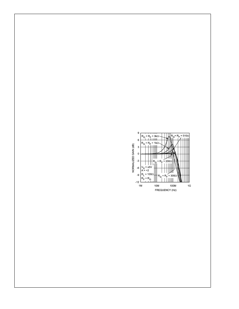
As an example of how important the component values are
for the behavior of your circuit, look at the following case: On
a board with good high frequency layout, an amplifier is
placed. For the two (equal) resistors in the feedback path, 5
different values are used to set the gain to +2. The resistors
vary from 200
to 3k
.
In
Figure 4
can be seen that there’s more peaking with
higher resistor values, which can lead to oscillations and bad
pulse responses. On the other hand the low resistor values
will contribute to higher overall power consumption.
NSC suggests the following evaluation boards as a guide for
high frequency layout and as an aid in device testing and
characterization.
Device
Package
Evaluation
Board PN
CLC730036
CLC730123
CLC730031
CLC730131
LMH6682MA
LMH6682MM
LMH6683MA
LMH6683MT
8-Pin SOIC
8-Pin MSOP
14-Pin SOIC
14-Pin TSSOP
These free evaluation boards are shipped when a device
sample request is placed with National Semiconductor.
20059063
FIGURE 4.
L
www.national.com
17
相關PDF資料 |
PDF描述 |
|---|---|
| LMH6683MA | 190MHz Single Supply, Dual and Triple Operational Amplifiers |
| LMH6683MAX | 190MHz Single Supply, Dual and Triple Operational Amplifiers |
| LMH6683MT | 190MHz Single Supply, Dual and Triple Operational Amplifiers |
| LMH6683MTX | 190MHz Single Supply, Dual and Triple Operational Amplifiers |
| LMH6702 | Ultra Low Distortion, Wideband Op Amp |
相關代理商/技術參數 |
參數描述 |
|---|---|
| LMH6683MA | 功能描述:運算放大器 - 運放 RoHS:否 制造商:STMicroelectronics 通道數量:4 共模抑制比(最小值):63 dB 輸入補償電壓:1 mV 輸入偏流(最大值):10 pA 工作電源電壓:2.7 V to 5.5 V 安裝風格:SMD/SMT 封裝 / 箱體:QFN-16 轉換速度:0.89 V/us 關閉:No 輸出電流:55 mA 最大工作溫度:+ 125 C 封裝:Reel |
| LMH6683MA/NOPB | 功能描述:運算放大器 - 運放 RoHS:否 制造商:STMicroelectronics 通道數量:4 共模抑制比(最小值):63 dB 輸入補償電壓:1 mV 輸入偏流(最大值):10 pA 工作電源電壓:2.7 V to 5.5 V 安裝風格:SMD/SMT 封裝 / 箱體:QFN-16 轉換速度:0.89 V/us 關閉:No 輸出電流:55 mA 最大工作溫度:+ 125 C 封裝:Reel |
| LMH6683MAX | 功能描述:運算放大器 - 運放 RoHS:否 制造商:STMicroelectronics 通道數量:4 共模抑制比(最小值):63 dB 輸入補償電壓:1 mV 輸入偏流(最大值):10 pA 工作電源電壓:2.7 V to 5.5 V 安裝風格:SMD/SMT 封裝 / 箱體:QFN-16 轉換速度:0.89 V/us 關閉:No 輸出電流:55 mA 最大工作溫度:+ 125 C 封裝:Reel |
| LMH6683MAX/NOPB | 功能描述:運算放大器 - 運放 RoHS:否 制造商:STMicroelectronics 通道數量:4 共模抑制比(最小值):63 dB 輸入補償電壓:1 mV 輸入偏流(最大值):10 pA 工作電源電壓:2.7 V to 5.5 V 安裝風格:SMD/SMT 封裝 / 箱體:QFN-16 轉換速度:0.89 V/us 關閉:No 輸出電流:55 mA 最大工作溫度:+ 125 C 封裝:Reel |
| LMH6683MT | 功能描述:運算放大器 - 運放 RoHS:否 制造商:STMicroelectronics 通道數量:4 共模抑制比(最小值):63 dB 輸入補償電壓:1 mV 輸入偏流(最大值):10 pA 工作電源電壓:2.7 V to 5.5 V 安裝風格:SMD/SMT 封裝 / 箱體:QFN-16 轉換速度:0.89 V/us 關閉:No 輸出電流:55 mA 最大工作溫度:+ 125 C 封裝:Reel |
發布緊急采購,3分鐘左右您將得到回復。