- 您現在的位置:買賣IC網 > PDF目錄361040 > LMH6702 (National Semiconductor Corporation) Ultra Low Distortion, Wideband Op Amp PDF資料下載
參數資料
| 型號: | LMH6702 |
| 廠商: | National Semiconductor Corporation |
| 英文描述: | Ultra Low Distortion, Wideband Op Amp |
| 中文描述: | 超低失真,寬帶運算放大器 |
| 文件頁數: | 9/13頁 |
| 文件大小: | 439K |
| 代理商: | LMH6702 |
Application Section
FEEDBACK RESISTOR
The LMH6702 achieves its excellent pulse and distortion
performance by using the current feedback topology. The
loop gain for a current feedback op amp, and hence the
frequency response, is predominantly set by the feedback
resistor value. The LMH6702 is optimized for use with a
237
feedback resistor. Using lower values can lead to
excessive ringing in the pulse response while a higher value
will limit the bandwidth. Application Note OA-13 discusses
this in detail along with the occasions where a different R
F
might be advantageous.
HARMONIC DISTORTION
The LMH6702 has been optimized for exceptionally low
harmonic distortion while driving very demanding resistive or
capacitive loads. Generally, when used as the input amplifier
to very high speed flash ADCs, the distortions introduced by
the converter will dominate over the low LMH6702 distor-
tions shown in the Typical Performance Characteristics sec-
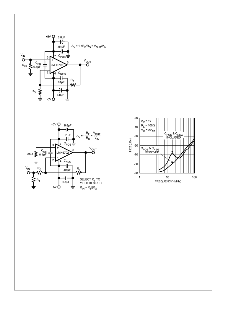
tion. The capacitor C
, shown across the supplies in
Figure
1
and
Figure 2
, is critical to achieving the lowest 2
nd
har-
monic distortion. For absolute minimum distortion levels, it is
also advisable to keep the supply decoupling currents
(ground connections to C
, and C
in
Figure 1
and
Figure 2
) separate from the ground connections to sensitive
input circuitry (such as R
G
, R
T
, and R
IN
ground connections).
Splitting the ground plane in this fashion and separately
routing the high frequency current spikes on the decoupling
caps back to the power supply (similar to "Star Connection"
layout technique) ensures minimum coupling back to the
input circuitry and results in best harmonic distortion re-
sponse (especially 2
nd
order distortion).
If this lay out technique has not been observed on a particu-
lar application board, designer may actually find that supply
decoupling caps could adversely affect HD2 performance by
increasing the coupling phenomenon already mentioned.
Figure 3
below shows actual HD2 data on a board where the
ground plane is "shared" between the supply decoupling
capacitors and the rest of the circuit. Once these capacitors
are removed, the HD2 distortion levels reduce significantly,
especially between 10MHz-20MHz, as shown in
Figure 3
below:
At these extremely low distortion levels, the high frequency
behavior of decoupling capacitors themselves could be sig-
nificant. In general, lower value decoupling caps tend to
have higher resonance frequencies making them more ef-
fective for higher frequency regions. A particular application
board which has been laid out correctly with ground returns
"split" to minimize coupling, would benefit the most by having
low value and higher value capacitors paralleled to take
advantage of the effective bandwidth of each and extend low
distortion frequency range.
Another important variable in getting the highest fidelity sig-
nal from the LMH6702 is the package itself. As already
noted, coupling between high frequency current transients
on supply lines and the device input can lead to excess
harmonic distortion.An important source of this coupling is in
fact through the device bonding wires. A smaller package, in
general, will have shorter bonding wires and therefore lower
coupling. This is true in the case of the SOT23-5 compared
to the SOIC package where a marked improvement in HD
can be measured in the SOT23-5 package.
Figure 4
below
shows the HD comparing SOT23-5 to SOIC package:
20039028
FIGURE 1. Recommended Non-Inverting Gain Circuit
20039027
FIGURE 2. Recommended Inverting Gain Circuit
20039022
FIGURE 3. Decoupling Current Adverse Effect on a
Board with Shared Ground Plane
L
www.national.com
9
相關PDF資料 |
PDF描述 |
|---|---|
| LMH6702MA | Ultra Low Distortion, Wideband Op Amp |
| LMH6702MAX | Ultra Low Distortion, Wideband Op Amp |
| LMH6702MF | Ultra Low Distortion, Wideband Op Amp |
| LMH6702MFX | Ultra Low Distortion, Wideband Op Amp |
| LMH6715 | Dual Wideband Video Op Amp |
相關代理商/技術參數 |
參數描述 |
|---|---|
| LMH6702JFLQMLV | 制造商:TI 制造商全稱:Texas Instruments 功能描述:1.7 GHz, Ultra Low Distortion, Wideband Op Amp |
| LMH6702JFQMLV | 功能描述:運算放大器 - 運放 RoHS:否 制造商:STMicroelectronics 通道數量:4 共模抑制比(最小值):63 dB 輸入補償電壓:1 mV 輸入偏流(最大值):10 pA 工作電源電壓:2.7 V to 5.5 V 安裝風格:SMD/SMT 封裝 / 箱體:QFN-16 轉換速度:0.89 V/us 關閉:No 輸出電流:55 mA 最大工作溫度:+ 125 C 封裝:Reel |
| LMH6702J-QMLV | 功能描述:運算放大器 - 運放 RoHS:否 制造商:STMicroelectronics 通道數量:4 共模抑制比(最小值):63 dB 輸入補償電壓:1 mV 輸入偏流(最大值):10 pA 工作電源電壓:2.7 V to 5.5 V 安裝風格:SMD/SMT 封裝 / 箱體:QFN-16 轉換速度:0.89 V/us 關閉:No 輸出電流:55 mA 最大工作溫度:+ 125 C 封裝:Reel |
| LMH6702MA | 功能描述:運算放大器 - 運放 RoHS:否 制造商:STMicroelectronics 通道數量:4 共模抑制比(最小值):63 dB 輸入補償電壓:1 mV 輸入偏流(最大值):10 pA 工作電源電壓:2.7 V to 5.5 V 安裝風格:SMD/SMT 封裝 / 箱體:QFN-16 轉換速度:0.89 V/us 關閉:No 輸出電流:55 mA 最大工作溫度:+ 125 C 封裝:Reel |
| LMH6702MA/NOPB | 功能描述:運算放大器 - 運放 Sgl Low Distort 600 Mhz Amp RoHS:否 制造商:STMicroelectronics 通道數量:4 共模抑制比(最小值):63 dB 輸入補償電壓:1 mV 輸入偏流(最大值):10 pA 工作電源電壓:2.7 V to 5.5 V 安裝風格:SMD/SMT 封裝 / 箱體:QFN-16 轉換速度:0.89 V/us 關閉:No 輸出電流:55 mA 最大工作溫度:+ 125 C 封裝:Reel |
發布緊急采購,3分鐘左右您將得到回復。