- 您現在的位置:買賣IC網 > PDF目錄361042 > LMV248LQ (NATIONAL SEMICONDUCTOR CORP) Dual Band GSM Power Controller PDF資料下載
參數資料
| 型號: | LMV248LQ |
| 廠商: | NATIONAL SEMICONDUCTOR CORP |
| 元件分類: | 通信及網絡 |
| 英文描述: | Dual Band GSM Power Controller |
| 中文描述: | SPECIALTY TELECOM CIRCUIT, CQCC16 |
| 封裝: | 4 X 4 MM, 0.80 MM HEIGHT, LLP-16 |
| 文件頁數: | 8/11頁 |
| 文件大小: | 289K |
| 代理商: | LMV248LQ |
Application Section
(Continued)
dependency of the external detector diodes is cancelled.
(Adding the temperature correction to the non-inverting ter-
minal is identical to subtracting the temperature correction
from the inverting terminal). The 10μA current sinks con-
nected to the signal paths for VfA, VfB, and TC provide a
bias current for the detector and temperature compensation
diodes. An approximate 200mV deadband for the Ramp
signal is preset.
Ramp Signal
The Ramp signal, which is positive going and ground refer-
enced, is the reference for the closed loop RF output control.
The Ramp signal is smoothed by internal filter with a corner
frequency of approximately 1.6MHz, formed from a 20k
resistor and 5pF capacitor. This filter eliminates step discon-
tinuities at the baseband DAC’s output. Transconductance
amplifier A2 provides current sinking proportional to the
Ramp signal.
Since the output of A2 connects to the inverting terminal of
A1, A1 draws current from VfA or VfB through the 48.5k
series resistance previously mentioned. This reduces the
voltage seen at the inverting terminal by the voltage drop
across the 48.5k
series resistance. The transconductance
of A2 is 1/(20k
). The net differential signal between the
non-inverting and inverting terminals of the error amplifier is
2.42 x Ramp-(Vf-TC). This means that the average (Vf-TC)
will be regulated to 2.42 x Ramp and that we want to choose
the RF directional coupler so that the peak RF detector
output at the maximum Ramp satisfies: (Peak Vf)-TC
≤
2.42
x (maximum Ramp). See “Selecting Coupler/Detector” in the
next section. Note that the
recommended
maximum Ramp
≤
2V.
V
HOME
Amplifier A3 and the diode D1 at its output clamp the low
value of the active output to the value set by V
HOME
, when-
ever the outputs are enabled by Tx_En. V
the inverting input of amplifier A3. The non-inverting input of
amplifier A3 connects to the active output selected by BS,
selection being done by analog switches. Also connecting to
the non-inverting input of amplifier A3 is a voltage divider.
This makes the equation for the minimum output voltage 3.0
x V
HOME
.
Outputs
The output amplifiers A4 and A5 are rail-to-rail complemen-
tary MOS output stages using Class AB control, and capable
of both sourcing and sinking current. The output amplifier not
selected by BS is disabled; both output amplifiers are dis-
abled when Tx_En is low. This conserves power.
The
single
compensation/stabilization
Comp1 and Comp2 is switched across the correct output
amplifier by analog switches controlled by BS.
network
across
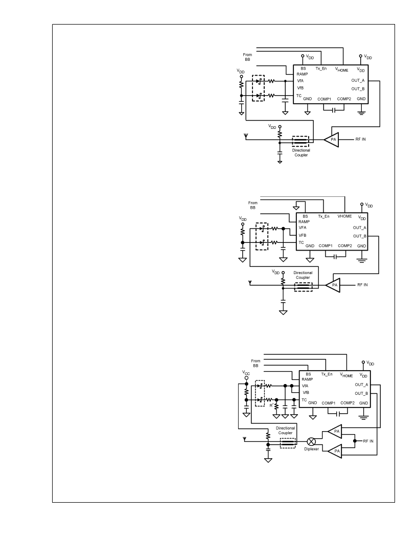
Typical LMV248 Configurations:
10137211
FIGURE 3. One Input, One Output (A)
10137212
FIGURE 4. One Input, One Output (B)
10137213
FIGURE 5. One Input, Two Outputs
L
www.national.com
8
相關PDF資料 |
PDF描述 |
|---|---|
| LMV248 | Dual Band GSM Power Controller |
| LMV248LQX | Electrical Tape; Peak Reflow Compatible (260 C):No RoHS Compliant: Yes |
| LMV324M | General Purpose, Low Voltage, Rail-to-Rail Output Operational Amplifiers |
| LMV324MT | General Purpose, Low Voltage, Rail-to-Rail Output Operational Amplifiers |
| LMV324MTX | General Purpose, Low Voltage, Rail-to-Rail Output Operational Amplifiers |
相關代理商/技術參數 |
參數描述 |
|---|---|
| LMV248LQX | 制造商:NSC 制造商全稱:National Semiconductor 功能描述:Dual Band GSM Power Controller |
| LMV2F-3M4 | 制造商:BACO Controls Inc 功能描述: |
| LMV301 | 制造商:ONSEMI 制造商全稱:ON Semiconductor 功能描述:Low Bias Current, 1.8V to 5V Single-Supply, Rail-to-Rail Operational Amplifier |
| LMV301MG | 功能描述:運算放大器 - 運放 RoHS:否 制造商:STMicroelectronics 通道數量:4 共模抑制比(最小值):63 dB 輸入補償電壓:1 mV 輸入偏流(最大值):10 pA 工作電源電壓:2.7 V to 5.5 V 安裝風格:SMD/SMT 封裝 / 箱體:QFN-16 轉換速度:0.89 V/us 關閉:No 輸出電流:55 mA 最大工作溫度:+ 125 C 封裝:Reel |
| LMV301MG/NOPB | 功能描述:運算放大器 - 運放 1.8V Low Ib Rro Sngl Op Amp RoHS:否 制造商:STMicroelectronics 通道數量:4 共模抑制比(最小值):63 dB 輸入補償電壓:1 mV 輸入偏流(最大值):10 pA 工作電源電壓:2.7 V to 5.5 V 安裝風格:SMD/SMT 封裝 / 箱體:QFN-16 轉換速度:0.89 V/us 關閉:No 輸出電流:55 mA 最大工作溫度:+ 125 C 封裝:Reel |
發布緊急采購,3分鐘左右您將得到回復。