- 您現(xiàn)在的位置:買賣IC網(wǎng) > PDF目錄361043 > LMV931MFX (NATIONAL SEMICONDUCTOR CORP) 1.8V, RRIO Operational Amplifiers PDF資料下載
參數(shù)資料
| 型號(hào): | LMV931MFX |
| 廠商: | NATIONAL SEMICONDUCTOR CORP |
| 元件分類: | 運(yùn)動(dòng)控制電子 |
| 英文描述: | 1.8V, RRIO Operational Amplifiers |
| 中文描述: | OP-AMP, 6000 uV OFFSET-MAX, 1.4 MHz BAND WIDTH, PDSO5 |
| 封裝: | SOT-23, 5 PIN |
| 文件頁數(shù): | 13/19頁 |
| 文件大小: | 625K |
| 代理商: | LMV931MFX |
Application Note
1.0 INPUT AND OUTPUT STAGE
The rail-to-rail input stage of this family provides more flex-
ibility for the designer. The LMV931/LMV932/LMV934 use a
complimentary PNP and NPN input stage in which the PNP
stage senses common mode voltage near V
and the NPN
stage senses common mode voltage near V
+
. The transition
from the PNP stage to NPN stage occurs 1V below V
+
. Since
both input stages have their own offset voltage, the offset of
the amplifier becomes a function of the input common mode
voltage and has a crossover point at 1V below V
+
.
This V
OS
crossover point can create problems for both DC
and AC coupled signals if proper care is not taken. Large
input signals that include the V
crossover point will cause
distortion in the output signal. One way to avoid such distor-
tion is to keep the signal away from the crossover. For
example, in a unity gain buffer configuration and with V
=
5V, a 5V peak-to-peak signal will contain input-crossover
distortion while a 3V peak-to-peak signal centered at 1.5V
will not contain input-crossover distortion as it avoids the
crossover point. Another way to avoid large signal distortion
is to use a gain of 1 circuit which avoids any voltage
excursions at the input terminals of the amplifier. In that
circuit, the common mode DC voltage can be set at a level
away from the V
OS
cross-over point. For small signals, this
transition in V
shows up as a V
dependent spurious
signal in series with the input signal and can effectively
degrade small signal parameters such as gain and common
mode rejection ratio. To resolve this problem, the small
signal should be placed such that it avoids the V
cross-
over point. In addition to the rail-to-rail performance, the
output stage can provide enough output current to drive
600
loads. Because of the high current capability, care
should be taken not to exceed the 150C maximum junction
temperature specification.
2.0 INPUT BIAS CURRENT CONSIDERATION
The LMV931/LMV932/LMV934 family has a complementary
bipolar input stage. The typical input bias current (I
B
) is
15nA. The input bias current can develop a significant offset
voltage. This offset is primarily due to I
flowing through the
negative feedback resistor, R
. For example, if I
is 50nA
and R
is 100k
, then an offset voltage of 5mV will develop
(V
= I
B
x R
). Using a compensation resistor (R
), as
shown in
Figure 1
, cancels this effect. But the input offset
current (I
) will still contribute to an offset voltage in the
same manner.
Typical Applications
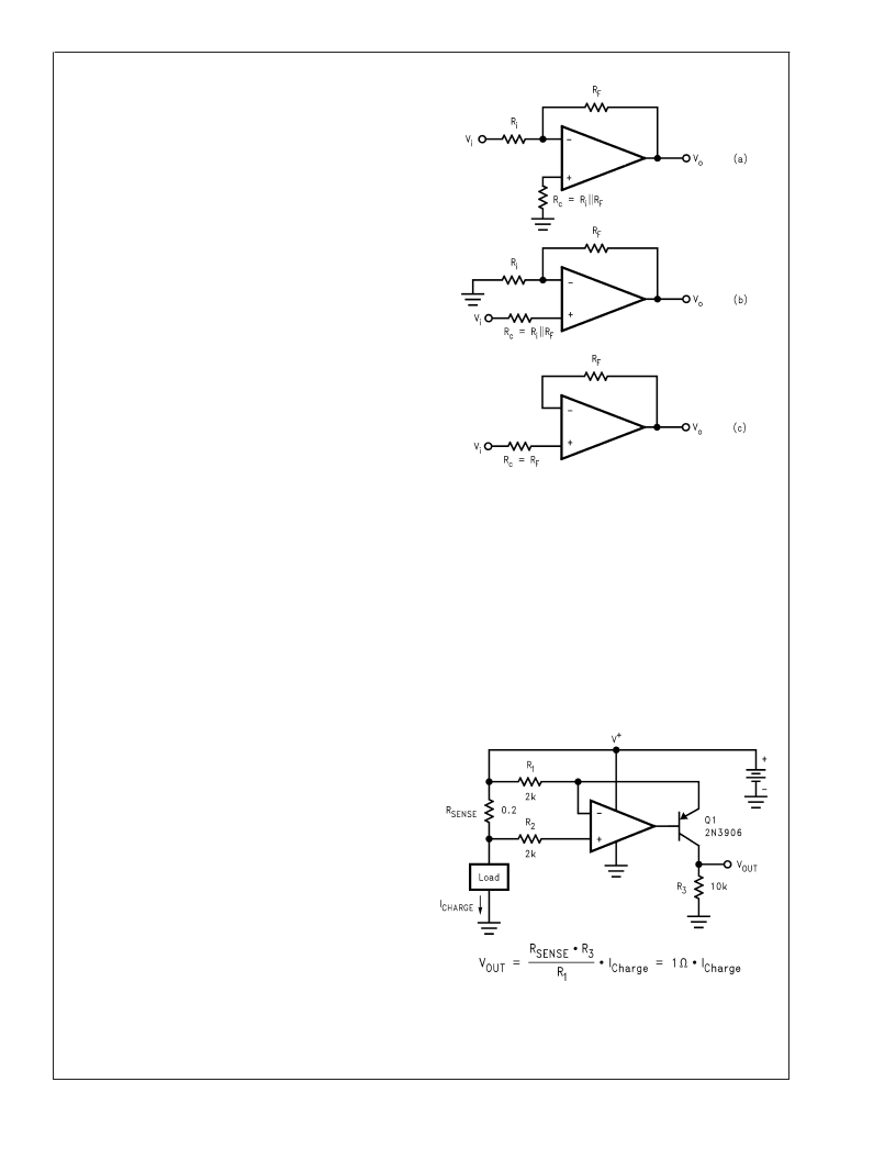
3.0 HIGH SIDE CURRENT SENSING
The high side current sensing circuit (
Figure 2
) is commonly
used in a battery charger to monitor charging current to
prevent over charging.Asense resistor R
is connected
to the battery directly. This system requires an op amp with
rail-to-rail input. The LMV931/LMV932/LMV934 are ideal for
this application because its common mode input range goes
up to the rail.
20032659
FIGURE 1. Canceling the Offset Voltage due to Input
Bias Current
200326H0
FIGURE 2. High Side Current Sensing
L
www.national.com
13
相關(guān)PDF資料 |
PDF描述 |
|---|---|
| LMV931MG | 1.8V, RRIO Operational Amplifiers |
| LMV931MGX | 1.8V, RRIO Operational Amplifiers |
| LMV932 | 1.8V, RRIO Operational Amplifiers |
| LMX2240M | Intermediate Frequency Receiver |
| LMX2240 | Crimp Tool for Power Connectors, Male; For Use With:Molex Pitch Sabre Terminals; Wire Size (AWG):18-14 |
相關(guān)代理商/技術(shù)參數(shù) |
參數(shù)描述 |
|---|---|
| LMV931MFX/E7002670 | 制造商:Texas Instruments 功能描述: |
| LMV931MFX/NOPB | 功能描述:運(yùn)算放大器 - 運(yùn)放 RoHS:否 制造商:STMicroelectronics 通道數(shù)量:4 共模抑制比(最小值):63 dB 輸入補(bǔ)償電壓:1 mV 輸入偏流(最大值):10 pA 工作電源電壓:2.7 V to 5.5 V 安裝風(fēng)格:SMD/SMT 封裝 / 箱體:QFN-16 轉(zhuǎn)換速度:0.89 V/us 關(guān)閉:No 輸出電流:55 mA 最大工作溫度:+ 125 C 封裝:Reel |
| LMV931MG | 功能描述:運(yùn)算放大器 - 運(yùn)放 RoHS:否 制造商:STMicroelectronics 通道數(shù)量:4 共模抑制比(最小值):63 dB 輸入補(bǔ)償電壓:1 mV 輸入偏流(最大值):10 pA 工作電源電壓:2.7 V to 5.5 V 安裝風(fēng)格:SMD/SMT 封裝 / 箱體:QFN-16 轉(zhuǎn)換速度:0.89 V/us 關(guān)閉:No 輸出電流:55 mA 最大工作溫度:+ 125 C 封裝:Reel |
| LMV931MG/NOPB | 功能描述:運(yùn)算放大器 - 運(yùn)放 RRIO 1.8V SGL OPAMP RoHS:否 制造商:STMicroelectronics 通道數(shù)量:4 共模抑制比(最小值):63 dB 輸入補(bǔ)償電壓:1 mV 輸入偏流(最大值):10 pA 工作電源電壓:2.7 V to 5.5 V 安裝風(fēng)格:SMD/SMT 封裝 / 箱體:QFN-16 轉(zhuǎn)換速度:0.89 V/us 關(guān)閉:No 輸出電流:55 mA 最大工作溫度:+ 125 C 封裝:Reel |
| LMV931MG/NOPB | 制造商:Texas Instruments 功能描述:Operational Amplifier (Op-Amp) IC |
發(fā)布緊急采購,3分鐘左右您將得到回復(fù)。