- 您現(xiàn)在的位置:買賣IC網(wǎng) > PDF目錄361044 > LMX2301TM (NATIONAL SEMICONDUCTOR CORP) PLLatinumTM 160 MHz Frequency Synthesizer for RF Personal Communications PDF資料下載
參數(shù)資料
| 型號: | LMX2301TM |
| 廠商: | NATIONAL SEMICONDUCTOR CORP |
| 元件分類: | XO, clock |
| 英文描述: | PLLatinumTM 160 MHz Frequency Synthesizer for RF Personal Communications |
| 中文描述: | PLL FREQUENCY SYNTHESIZER, 160 MHz, PDSO20 |
| 封裝: | 0.173 INCH, PLASTIC, TSSOP-20 |
| 文件頁數(shù): | 2/14頁 |
| 文件大小: | 225K |
| 代理商: | LMX2301TM |
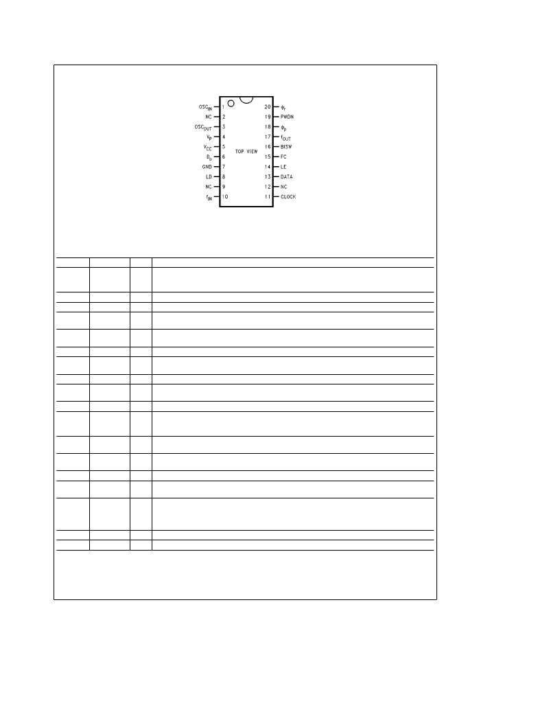
Connection Diagram
LMX2301
TL/W/12458–2
20-Lead (0.173
×
Wide) Thin Shrink
Small Outline Package (TM)
Order Number LMX2301TM or LMX2301TMX
See NS Package Number MTC20
Pin Descriptions
Pin No.
Pin Name
I/O
Description
1
OSC
IN
I
Oscillator input. A CMOS inverting gate input intended for connection to a crystal resonator for
operation as an oscillator. The input has a V
CC
/2 input threshold and can be driven from an
external CMOS or TTL logic gate. May also be from a reference oscillator.
3
OSC
OUT
V
P
V
CC
O
Oscillator output.
Power supply for charge pump. Must be
t
V
CC
.
Power supply voltage input. Input may range from 2.7V to 5.5V. Bypass capacitors should be
placed as close as possible to this pin and be connected directly to the ground plane.
4
5
6
D
o
O
Internal charge pump output. For connection to a loop filter for driving the input of an external
VCO.
7
GND
Ground.
8
LD
O
Lock detect. Output provided to indicate when the VCO frequency is in ‘‘lock’’. When the loop is
locked, the pin’s output is HIGH with narrow low pulses.
10
f
IN
CLOCK
I
RF buffer input. Small signal input from the VCO.
11
I
High impedance CMOS Clock input. Data is clocked in on the rising edge, into the various
counters and registers.
13
DATA
I
Binary serial data input. Data entered MSB first. LSB is control bit. High impedance CMOS input.
14
LE
I
Load enable input (with internal pull-up resistor). When LE transitions HIGH, data stored in the
shift registers is loaded into the appropriate latch (control bit dependent). Clock must be low
when LE toggles high or low. See Serial Data Input Timing Diagram.
15
FC
I
Phase control select (with internal pull-up resistor). When FC is LOW, the polarity of the phase
comparator and charge pump combination is reversed.
16
BISW
O
Analog switch output. When LE is HIGH, the analog switch is ON, routing the internal charge
pump output through BISW (as well as through D
o
).
Monitor pin of phase comparator input. CMOS output.
17
f
OUT
w
p
O
18
O
Output for external charge pump.
w
p
is an open drain N-channel transistor and requires a pull-up
resistor.
19
PWDN
I
Power Down (with internal pull-up resistor).
PWDN
e
HIGH for normal operation.
PWDN
e
LOW for power saving.
Power down function is gated by the return of the charge pump to a TRI-STATE condition.
20
w
r
NC
O
Output for external charge pump.
w
r
is a CMOS logic output.
No connect.
2,9,12
http://www.national.com
2
相關(guān)PDF資料 |
PDF描述 |
|---|---|
| LMX2301TMX | PLLatinumTM 160 MHz Frequency Synthesizer for RF Personal Communications |
| LMX2305TM | PLLatinumTM 550 MHz Frequency Synthesizer for RF Personal Communications |
| LMX2305TMX | PLLatinumTM 550 MHz Frequency Synthesizer for RF Personal Communications |
| LMX2305 | PLLatinum 550 MHz Frequency Synthesizer for RF Personal Communications(PLLatinum技術(shù)用于射頻個人通訊的550MHZ頻率合成器) |
| LMX2354TM | PLLatinum Fractional N RF/ Integer N IF Dual Low Power Frequency Synthesizer |
相關(guān)代理商/技術(shù)參數(shù) |
參數(shù)描述 |
|---|---|
| LMX2301TMX | 制造商:NSC 制造商全稱:National Semiconductor 功能描述:PLLatinumTM 160 MHz Frequency Synthesizer for RF Personal Communications |
| LMX2305 | 制造商:NSC 制造商全稱:National Semiconductor 功能描述:PLLatinumTM 550 MHz Frequency Synthesizer for RF Personal Communications |
| LMX2305 WAF | 制造商:Texas Instruments 功能描述: |
| LMX2305C WAF | 制造商:Texas Instruments 功能描述: |
| LMX2305TM | 制造商:Rochester Electronics LLC 功能描述: |
發(fā)布緊急采購,3分鐘左右您將得到回復(fù)。