- 您現在的位置:買賣IC網 > PDF目錄361044 > LMX9820ASMX (NATIONAL SEMICONDUCTOR CORP) Bluetooth Serial Port Module PDF資料下載
參數資料
| 型號: | LMX9820ASMX |
| 廠商: | NATIONAL SEMICONDUCTOR CORP |
| 元件分類: | 通信及網絡 |
| 英文描述: | Bluetooth Serial Port Module |
| 中文描述: | SPECIALTY TELECOM CIRCUIT, PBGA116 |
| 封裝: | 10.10 X 14.10 MM, 2 MM HEIGHT, LGA-116 |
| 文件頁數: | 18/44頁 |
| 文件大小: | 579K |
| 代理商: | LMX9820ASMX |
第1頁第2頁第3頁第4頁第5頁第6頁第7頁第8頁第9頁第10頁第11頁第12頁第13頁第14頁第15頁第16頁第17頁當前第18頁第19頁第20頁第21頁第22頁第23頁第24頁第25頁第26頁第27頁第28頁第29頁第30頁第31頁第32頁第33頁第34頁第35頁第36頁第37頁第38頁第39頁第40頁第41頁第42頁第43頁第44頁
www.national.com
18
Revision 1.0
L
8.0 Digital Smart Radio
(Continued)
pendent of input waveform duty cycle or amplitude varia-
tions. Loop lockup occurs when all the negative transitions
on the inputs, F_REF and F_MOD, coincide. Both outputs
(i.e., Up and Down) then remain high. This is equal to the
zero error mode. The phase-frequency detector input fre-
quency range operates at 12 MHz.
8.6 TRANSMITTER CIRCUITRY
The transmitter consists of ROM tables, two Digital to Ana-
log (DA) converters, two low-pass filters, IQ mixers, and a
power amplifier (PA).
The ROM tables generate a digital IQ signal based on the
transmit data. The output of the ROM tables is inserted into
IQ-DA converters and filtered through two low-pass filters.
The two signal components are mixed up to 2.5 GHz by the
TX mixers and added together before being inserted into
the transmit PA.
8.6.1 IQ-DA Converters and TX Mixers
The ROM output signals drive an I- and Q-DA converter.
Two Butterworth low-pass filters filter the DA output signals.
The 6 MHz clock for the DA converters and the logic circuit-
ry around the ROM tables are derived from the autotuner.
The TX mixers mix the balanced I- and Q-signals up to 2.4-
2.5 GHz. The output signals of the I- and Q-mixers are
summed.
8.7 CRYSTAL REQUIREMENTS
The LMX9820A includes a crystal driver circuit. This circuit
operates with an external crystal and capacitors to form an
oscillator. Figure 10 shows the recommended crystal circuit.
Table 24 on page 22 specifies system clock requirements.
The RF local oscillator and internal digital clocks for the
LMX9820A are derived from the reference clock at the
CLK+ input. This reference may either come from an exter-
nal clock or a dedicated crystal oscillator. The crystal oscil-
lator connections require a crystal and two grounded
capacitors.
It is important to consider board- and design-dependent
capacitance in tuning the crystal circuit. The following
equations allow a close approximation of the required crys-
tal tuning capacitance, but the actual values will vary with
the capacitive properties of the board. As a result, there is
some fine tuning of the crystal circuit which cannot be cal-
culated, but must be determined experimentally by testing
different values of load capacitance.
Many different crystals can be used with the LMX9820A. A
key requirement from the Bluetooth specification is 20
ppm. Additionally, ESR (Equivalent Series Resistance)
must be carefully considered. LMX9820A can support a
maximum of 230
ESR, but it is recommended to stay <
100
ESR for best performance over voltage and tempera-
ture. See Figure 14 on page 22 for ESR as part of the crys-
tal circuit for more information.
8.7.1 Crystal
The crystal appears inductive near its resonant frequency.
It forms a resonant circuit with its load capacitors. The res-
onant frequency may be trimmed with the crystal load
capacitance.
1. Load Capacitance
For resonance at the correct frequency, the crystal should
be loaded with its specified load capacitance, which is the
value of capacitance used in conjunction with the crystal
unit. Load capacitance is a parameter specified by the
crystal, typically expressed in pF. The crystal circuit shown
in Figure 11 on page 19 is composed of:
— C1 (motional capacitance)
— R1 (motional resistance)
— L1 (motional inductance)
— C0 (static or shunt capacitance)
The LMX9820A provides some of the load with internal
capacitors C
int
. The remainder must come from the exter-
nal capacitors and tuning capacitors labeled Ct1 and Ct2
as shown in Figure 10. Ct1 and Ct2 should have the same
the value for best noise performance.
The LMX9820A has an additional internal capacitance
C
TUNE
of 2.6 pF. Crystal load capacitance (C
L)
is calculated
as:
C
L
= C
int
+ C
TUNE
+ Ct1/Ct2
The C
L
above does not include the crystal internal self-
capacitance C
0
as shown in Figure 11 on page 19, so the
total capacitance is:
C
total
= C
L
+ C
0
Based on the crystal specification and equation:
C
L
= C
int
+ C
TUNE
+ Ct1//Ct2
C
L
= 8pF + 2.6pF + 6pF = 16.6pF
16.6 pF is very close to the TEW crystal requirement of 16
pF load capacitance. With the internal shunt capacitance
C
total
:
C
total
= 16.6pF + 5pF = 21.6pF
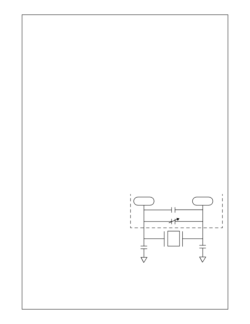
Figure 10. LMX9820A Crystal Recommended
Circuit
CLK+
CLK-
Ct1
Ct2
Crystal
LMX9820A
C
int
C
TUNE
相關PDF資料 |
PDF描述 |
|---|---|
| LMX9820A | Bluetooth Serial Port Module |
| LMX9820ASM | Bluetooth Serial Port Module |
| LMX9820 | Bluetooth Serial Port Module |
| LMX9820SB | Bluetooth Serial Port Module |
| LMX9820SBX | Bluetooth Serial Port Module |
相關代理商/技術參數 |
參數描述 |
|---|---|
| LMX9820ASMX/NOPB | 制造商:Texas Instruments 功能描述:Bluetooth Class II 3.3V 0.704Mbps 116-Pin LTCC T/R 制造商:Texas Instruments 功能描述:MODULE BLUETOOTH SERIAL PORT SMD |
| LMX9820SB | 制造商:Texas Instruments 功能描述: 制造商:Texas Instruments 功能描述:MODULE BLUE TOOTH 116-LTCC 制造商:Texas Instruments 功能描述:BLUETOOTH MODULE 2.4GHZ 704KBPS |
| LMX9820SBX | 制造商:NSC 制造商全稱:National Semiconductor 功能描述:Bluetooth Serial Port Module |
| LMX9830 | 制造商:NSC 制造商全稱:National Semiconductor 功能描述:BluetoothTM Serial Port Module |
| LMX9830DONGLE | 功能描述:藍牙/802.15.1 開發工具 LMX9830 BLUETOOTH EVAL KIT RoHS:否 制造商:Panasonic Electronic Components 產品:Bluetooth Evaluation Kit 工具用于評估:PAN1721 頻率:2.4 GHz 接口類型:I2C 工作電源電壓:2 V to 3.6 V |
發布緊急采購,3分鐘左右您將得到回復。