- 您現在的位置:買賣IC網 > PDF目錄361045 > LP3982IMM-2.77 (NATIONAL SEMICONDUCTOR CORP) Micropower, Ultra Low-Dropout, Low-Noise, 300mA CMOS Regulator PDF資料下載
參數資料
| 型號: | LP3982IMM-2.77 |
| 廠商: | NATIONAL SEMICONDUCTOR CORP |
| 元件分類: | 基準電壓源/電流源 |
| 英文描述: | Micropower, Ultra Low-Dropout, Low-Noise, 300mA CMOS Regulator |
| 中文描述: | 2.77 V FIXED POSITIVE LDO REGULATOR, 0.22 V DROPOUT, PDSO8 |
| 封裝: | MSOP-8 |
| 文件頁數: | 6/12頁 |
| 文件大小: | 361K |
| 代理商: | LP3982IMM-2.77 |
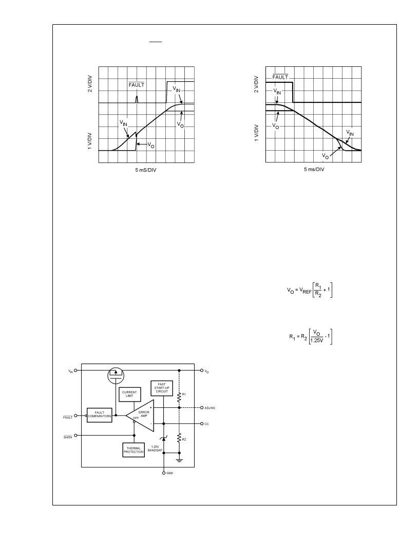
Typical Performance Characteristics
Unless otherwise specified, V
IN
= V
O
+ 0.5V, C
IN
= C
OUT
=
2.2μF, C
CC
= 33nF, T
J
= 25C, V
SHDN
= V
IN
. (Continued)
Power-Up Response
Power-Down Response
20036911
20036912
Application Information
General Information
LP3982 is package, pin and performance compatible with
Maxim’s MAX8860 excluding reverse battery protection and
Dual Mode
function (fixed and adjustable combined).
Figure 1
shows the functional block diagram for the LP3982.
A 1.25V bandgap reference, an error amplifier and a PMOS
pass transistor perform voltage regulation while being sup-
ported by shutdown, fault, and the usual Temperature and
current protection circuitry
The regulator’s topology is the classic type with negative
feedback from the output to one of the inputs of the error
amplifier. Feedback resistors R
and R
are either internal or
external to the IC, depending on whether it is the fixed
voltage version or the adjustable version. The negative feed-
back and high open loop gain of the error amplifier cause the
two inputs of the error amplifier to be virtually equal in
voltage. If the output voltage changes due to load changes,
the error amplifier provides the appropriate drive to the pass
transistor to maintain the error amplifier’s inputs as virtually
equal. In short, the error amplifier keeps the output voltage
constant in order to keep its inputs equal.
Output Voltage Setting (ADJ version only)
The output voltage is set according to the amount of nega-
tive feedback (Note that the pass transistor inverts the feed-
back signal.)
Figure 2
simplifies the topology of the LP3982.
This type of regulator can be represented as an op amp
configured as non-inverting amplifier and a fixed DC Voltage
(V
REF
) for its input signal. The special characteristic of this
op amp is its extra-large output transistor that only sources
current. In terms of its non-inverting configuration, the output
voltage equals V
REF
times the closed loop gain:
Utilize the following equation for adjusting the output to a
particular voltage:
Choose R
= 100k to optimize accuracy, power supply re-
jection, noise and power consumption.
20036913
FIGURE 1. Functional Block Diagram for the LP3982
L
www.national.com
6
相關PDF資料 |
PDF描述 |
|---|---|
| LP3982IMM-3.0 | Micropower, Ultra Low-Dropout, Low-Noise, 300mA CMOS Regulator |
| LP3982IMM-2.82 | Micropower, Ultra Low-Dropout, Low-Noise, 300mA CMOS Regulator |
| LP3982ILD-1.8 | Micropower, Ultra Low-Dropout, Low-Noise, 300mA CMOS Regulator |
| LP3982ILD-2.5 | Micropower, Ultra Low-Dropout, Low-Noise, 300mA CMOS Regulator |
| LP3982ILD-2.77 | Micropower, Ultra Low-Dropout, Low-Noise, 300mA CMOS Regulator |
相關代理商/技術參數 |
參數描述 |
|---|---|
| LP3982IMM282 | 制造商:Texas Instruments 功能描述: |
| LP3982IMM-3.0 | 功能描述:低壓差穩壓器 - LDO RoHS:否 制造商:Texas Instruments 最大輸入電壓:36 V 輸出電壓:1.4 V to 20.5 V 回動電壓(最大值):307 mV 輸出電流:1 A 負載調節:0.3 % 輸出端數量: 輸出類型:Fixed 最大工作溫度:+ 125 C 安裝風格:SMD/SMT 封裝 / 箱體:VQFN-20 |
| LP3982IMM-3.0 | 制造商:Texas Instruments 功能描述:V REG LDO 0.3A 3.0V 3982 MSOP8 |
| LP3982IMM-3.0/NOPB | 功能描述:低壓差穩壓器 - LDO RoHS:否 制造商:Texas Instruments 最大輸入電壓:36 V 輸出電壓:1.4 V to 20.5 V 回動電壓(最大值):307 mV 輸出電流:1 A 負載調節:0.3 % 輸出端數量: 輸出類型:Fixed 最大工作溫度:+ 125 C 安裝風格:SMD/SMT 封裝 / 箱體:VQFN-20 |
| LP3982IMM-3.3 | 功能描述:低壓差穩壓器 - LDO RoHS:否 制造商:Texas Instruments 最大輸入電壓:36 V 輸出電壓:1.4 V to 20.5 V 回動電壓(最大值):307 mV 輸出電流:1 A 負載調節:0.3 % 輸出端數量: 輸出類型:Fixed 最大工作溫度:+ 125 C 安裝風格:SMD/SMT 封裝 / 箱體:VQFN-20 |
發布緊急采購,3分鐘左右您將得到回復。