- 您現在的位置:買賣IC網 > PDF目錄361046 > LQA28A (National Semiconductor Corporation) 3V, 1W Boosted Boomer PDF資料下載
參數資料
| 型號: | LQA28A |
| 廠商: | National Semiconductor Corporation |
| 英文描述: | 3V, 1W Boosted Boomer |
| 中文描述: | 3V的,1W的,細看布瑪 |
| 文件頁數: | 15/18頁 |
| 文件大小: | 1063K |
| 代理商: | LQA28A |
Application Information
(Continued)
GENERAL MIXED-SIGNAL LAYOUT
RECOMMENDATION
This section provides practical guidelines for mixed signal
PCB layout that involves various digital/analog power and
ground traces. Designers should note that these are only
"rule-of-thumb" recommendations and the actual results will
depend heavily on the final layout.
Power and Ground Circuits
For 2 layer mixed signal design, it is important to isolate the
digital power and ground trace paths from the analog power
and ground trace paths. Star trace routing techniques (bring-
ing individual traces back to a central point rather than daisy
chaining traces together in a serial manner) can have a
major impact on low level signal performance. Star trace
routing refers to using individual traces to feed power and
ground to each circuit or even device. This technique will
take require a greater amount of design time but will not
increase the final price of the board. The only extra parts
required may be some jumpers.
Single-Point Power / Ground Connection
The analog power traces should be connected to the digital
traces through a single point (link). A "Pi-filter" can be helpful
in minimizing high frequency noise coupling between the
analog and digital sections. It is further recommended to
place digital and analog power traces over the correspond-
ing digital and analog ground traces to minimize noise cou-
pling.
Placement of Digital and Analog Components
All digital components and high-speed digital signals traces
should be located as far away as possible from analog
components and circuit traces.
Avoiding Typical Design / Layout Problems
Avoid ground loops or running digital and analog traces
parallel to each other (side-by-side) on the same PCB layer.
When traces must cross over each other do it at 90 degrees.
Running digital and analog traces at 90 degrees to each
other from the top to the bottom side as much as possible will
minimize capacitive noise coupling and crosstalk.
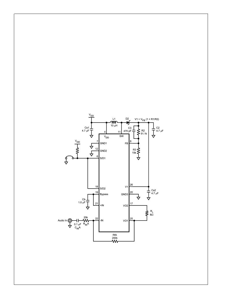
20126250
FIGURE 3. Demo Board Reference Schematic
L
www.national.com
15
相關PDF資料 |
PDF描述 |
|---|---|
| LV8572A | LV8572A Low Voltage Real Time Clock (RTC) |
| LV8572AM | LV8572A Low Voltage Real Time Clock (RTC) |
| LV8572AN | LV8572A Low Voltage Real Time Clock (RTC) |
| LV8573A | LV8573A Low Voltage Real Time Clock (RTC) |
| LV8573AM | LV8573A Low Voltage Real Time Clock (RTC) |
相關代理商/技術參數 |
參數描述 |
|---|---|
| LQA30A300C | 功能描述:整流器 Q-Series 300V 15A Dual Ultra-Low Qrr RoHS:否 制造商:Vishay Semiconductors 產品:Standard Recovery Rectifiers 配置: 反向電壓:100 V 正向電壓下降: 恢復時間:1.2 us 正向連續電流:2 A 最大浪涌電流:35 A 反向電流 IR:5 uA 安裝風格:SMD/SMT 封裝 / 箱體:DO-221AC 封裝:Reel |
| LQA30B200C | 功能描述:二極管 - 通用,功率,開關 200V, Dual, 15A Ultra-Low Qrr IC RoHS:否 制造商:STMicroelectronics 產品:Switching Diodes 峰值反向電壓:600 V 正向連續電流:200 A 最大浪涌電流:800 A 配置: 恢復時間:2000 ns 正向電壓下降:1.25 V 最大反向漏泄電流:300 uA 最大功率耗散: 工作溫度范圍: 安裝風格:SMD/SMT 封裝 / 箱體:ISOTOP 封裝:Tube |
| LQA30N200C | 功能描述:整流器 200V, Dual, 15A Ultra-Low Qrr IC RoHS:否 制造商:Power Integrations 產品: 配置: 反向電壓: 正向電壓下降: 恢復時間: 正向連續電流: 最大浪涌電流: 反向電流 IR: 安裝風格: 封裝 / 箱體: 封裝:Reel |
| LQA30T200C | 功能描述:整流器 200V, Dual, 15A Ultra-Low Qrr IC RoHS:否 制造商:Power Integrations 產品:Fast Recovery Rectifiers 配置:Dual 反向電壓:200 V 正向電壓下降:1.2 V 恢復時間:16.5 ns 正向連續電流:15 A 最大浪涌電流:130 A 反向電流 IR:500 uA 安裝風格:Through Hole 封裝 / 箱體:TO-220AB 封裝:Tube |
| LQA30T300 | 功能描述:整流器 Q-Series 300V 30A Ultra Low Qrr RoHS:否 制造商:Vishay Semiconductors 產品:Standard Recovery Rectifiers 配置: 反向電壓:100 V 正向電壓下降: 恢復時間:1.2 us 正向連續電流:2 A 最大浪涌電流:35 A 反向電流 IR:5 uA 安裝風格:SMD/SMT 封裝 / 箱體:DO-221AC 封裝:Reel |
發布緊急采購,3分鐘左右您將得到回復。