- 您現在的位置:買賣IC網 > Datasheet目錄42 > LTC4230CGN#TRPBF (Linear Technology)IC CONTRLLR HOT SWAP TRPL 20SSOP Datasheet資料下載
參數資料
| 型號: | LTC4230CGN#TRPBF |
| 廠商: | Linear Technology |
| 文件頁數: | 24/36頁 |
| 文件大小: | 384K |
| 描述: | IC CONTRLLR HOT SWAP TRPL 20SSOP |
| 標準包裝: | 2,500 |
| 類型: | 熱交換控制器 |
| 應用: | 通用 |
| 內部開關: | 無 |
| 電源電壓: | 1.7 V ~ 16.5 V |
| 工作溫度: | 0°C ~ 70°C |
| 安裝類型: | 表面貼裝 |
| 封裝/外殼: | 20-SSOP(0.154",3.90mm 寬) |
| 供應商設備封裝: | 20-SSOP |
| 包裝: | 帶卷 (TR) |
第1頁第2頁第3頁第4頁第5頁第6頁第7頁第8頁第9頁第10頁第11頁第12頁第13頁第14頁第15頁第16頁第17頁第18頁第19頁第20頁第21頁第22頁第23頁當前第24頁第25頁第26頁第27頁第28頁第29頁第30頁第31頁第32頁第33頁第34頁第35頁第36頁
24
LTC4230
4230f
maximum rating for V
GS
is typically ?0V for standard
MOSFETs. However, the V
GS
maximum rating for logic-
level MOSFETs ranges from ?V to ?0V depending upon
the manufacturer and the specific part number. The
LTC4230s gate overdrive as a function of V
CC
is illustrated
in the Typical Performance curves. Logic-level MOSFETs
are recommended for low supply voltage applications and
standard MOSFETs can be used for applications where
supply voltage is greater than 4.75V.
Note that in some applications, the gate of the external
MOSFET can discharge faster than the output voltage
when the circuit breaker is tripped. This causes a negative
V
GS
voltage on the external MOSFET. Usually, the selected
external MOSFET should have a 盫
GS(MAX)
rating that is
higher than the operating input supply voltage to ensure
that the external MOSFET is not destroyed by a negative
V
GS
voltage. In addition, the 盫
GS(MAX)
rating of the
MOSFET must be higher than the gate overdrive voltage.
Lower 盫
GS(MAX)
rating MOSFETs can be used with the
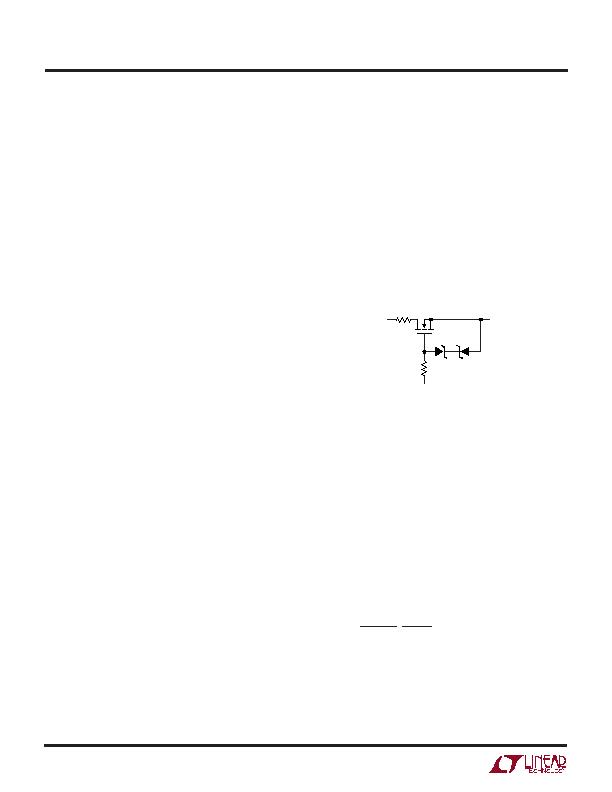
LTC4230 if the GATEn overdrive is clamped to a lower
voltage. The circuit in Figure 13 illustrates the use of zener
diodes to clamp the LTC4230s GATEn overdrive signal if
lower voltage MOSFETs are used.
The R
DS(ON)
of the external pass transistor should be low
to make its drain-source voltage (V
DS
) a small percentage
of V
CC
. At a V
CC
= 2.5V, V
DS
+ V
RSENSE
= 0.1V yields 4%
error at the output voltage. This restricts the choice of
MOSFETs to very low R
DS(ON)
. At higher V
CC
voltages, the
V
DS
requirement can be relaxed in which case MOSFET
package dissipation (P
D
and T
J
) may limit the value of
R
DS(ON)
. Table 5 lists some power MOSFETs that can be
used with the LTC4230.
Power MOSFET junction temperature is dependent on four
parameters: current delivered to the load, I
LOAD
, R
DS(ON)
,
junction-to-ambient thermal resistance, ?/DIV>
JA
, and the maxi-
mum ambient temperature to which the circuit will be
exposed, T
A(MAX)
. For reliable circuit operation, the maxi-
mum junction temperature (T
J(MAX)
) for a power MOSFET
should not exceed the manufacturers recommended value.
This includes normal mode operation, start-up, current-
limit and autoretry mode in a fault condition. For a given
set of conditions, the junction temperature of a power
MOSFET is given by Equation 13:
MOSFET Junction Temperature,
T
J(MAX)
d (T
A(MAX)
+ ?/DIV>
JA
" P
D
)
(13)
where
P
D
= (I
LOAD
)
2
" R
DS(ON)
PCB layout techniques for optimal thermal management
of power MOSFET power dissipation help to keep device
?/DIV>
JA
as low as possible. See the section on PCB Layout
Considerations for more information.
V
CC
V
OUT
*USER SELECTED VOLTAGE CLAMP
(A LOW BIAS CURRENT ZENER DIODE IS RECOMMENDED)
1N4688 (5V)
1N4692 (7V): LOGIC-LEVEL MOSFET
1N4695 (9V)
1N4702 (15V): STANDARD-LEVEL MOSFET
4230 F13
R
SENSE
R
G
200&
GATE
D1*
D2*
Q1
Figure 13. Optional Gate Clamp for Lower V
GS(MAX)
MOSFETs
USING STAGGERED PIN CONNECTORS
The LTC4230 can be used on either a printed circuit board
or on the backplane side of the connector, and examples
for both are shown in Figure 14. Printed circuit board edge
connectors with staggered pins are recommended as the
insertion and removal of circuit boards do sequence the
pin connections. Supply voltage and ground connections
on the printed circuit board should be wired to the edge
connectors long pins or blades. Control and status sig-
nals (like RESETn, FAULT and ON) passing through the
cards edge connector should be wired to short length pins
or blades.
APPLICATIO S I FOR ATIO
U
U
U
相關PDF資料 |
PDF描述 |
|---|---|
| LTC4232CDHC#TRPBF | IC CTLR HOT SWAP 5A 16-DFN |
| LTC4240IGN#TRPBF | IC CTRLR HOTSWAP CPCI I2C 28SSOP |
| LTC4241IGN#PBF | IC CTRLR HOTSWAP 3.3V AUX 20SSOP |
| LTC4242CUHF#TRPBF | IC CNTRLR HOT SWAP 38-QFN |
| LTC4244CGN-1#TRPBF | IC CTRLR HOTSWAP PCI 20-SSOP |
相關代理商/技術參數 |
參數描述 |
|---|---|
| LTC4230IGN | 功能描述:IC CONTRLLR HOT SWAP TRPL 20SSOP RoHS:否 類別:集成電路 (IC) >> PMIC - 熱交換 系列:- 產品培訓模塊:Lead (SnPb) Finish for COTS Obsolescence Mitigation Program 標準包裝:119 系列:- 類型:熱交換控制器 應用:通用型,PCI Express? 內部開關:無 電流限制:- 電源電壓:3.3V,12V 工作溫度:-40°C ~ 85°C 安裝類型:表面貼裝 封裝/外殼:80-TQFP 供應商設備封裝:80-TQFP(12x12) 包裝:托盤 產品目錄頁面:1423 (CN2011-ZH PDF) |
| LTC4230IGN#PBF | 功能描述:IC CONTRLLR HOT SWAP TRPL 20SSOP RoHS:是 類別:集成電路 (IC) >> PMIC - 熱交換 系列:- 產品培訓模塊:Lead (SnPb) Finish for COTS Obsolescence Mitigation Program 標準包裝:119 系列:- 類型:熱交換控制器 應用:通用型,PCI Express? 內部開關:無 電流限制:- 電源電壓:3.3V,12V 工作溫度:-40°C ~ 85°C 安裝類型:表面貼裝 封裝/外殼:80-TQFP 供應商設備封裝:80-TQFP(12x12) 包裝:托盤 產品目錄頁面:1423 (CN2011-ZH PDF) |
| LTC4230IGN#TR | 功能描述:IC CONTRLLR HOT SWAP TRPL 20SSOP RoHS:否 類別:集成電路 (IC) >> PMIC - 熱交換 系列:- 產品培訓模塊:Lead (SnPb) Finish for COTS Obsolescence Mitigation Program 標準包裝:119 系列:- 類型:熱交換控制器 應用:通用型,PCI Express? 內部開關:無 電流限制:- 電源電壓:3.3V,12V 工作溫度:-40°C ~ 85°C 安裝類型:表面貼裝 封裝/外殼:80-TQFP 供應商設備封裝:80-TQFP(12x12) 包裝:托盤 產品目錄頁面:1423 (CN2011-ZH PDF) |
| LTC4230IGN#TRPBF | 功能描述:IC CONTRLLR HOT SWAP TRPL 20SSOP RoHS:是 類別:集成電路 (IC) >> PMIC - 熱交換 系列:- 產品培訓模塊:Lead (SnPb) Finish for COTS Obsolescence Mitigation Program 標準包裝:119 系列:- 類型:熱交換控制器 應用:通用型,PCI Express? 內部開關:無 電流限制:- 電源電壓:3.3V,12V 工作溫度:-40°C ~ 85°C 安裝類型:表面貼裝 封裝/外殼:80-TQFP 供應商設備封裝:80-TQFP(12x12) 包裝:托盤 產品目錄頁面:1423 (CN2011-ZH PDF) |
| LTC4232CDHC#PBF | 功能描述:IC CTLR HOT SWAP 5A 16-DFN RoHS:是 類別:集成電路 (IC) >> PMIC - 熱交換 系列:- 產品培訓模塊:Obsolescence Mitigation Program 標準包裝:100 系列:- 類型:熱插拔開關 應用:通用 內部開關:是 電流限制:可調 電源電壓:9 V ~ 13.2 V 工作溫度:-40°C ~ 150°C 安裝類型:表面貼裝 封裝/外殼:10-WFDFN 裸露焊盤 供應商設備封裝:10-TDFN-EP(3x3) 包裝:管件 |
發布緊急采購,3分鐘左右您將得到回復。