- 您現在的位置:買賣IC網 > Datasheet目錄42 > LTC4350IGN#PBF (Linear Technology)IC CTLR HOTSWAP LOADSHARE 16SSOP Datasheet資料下載
參數資料
| 型號: | LTC4350IGN#PBF |
| 廠商: | Linear Technology |
| 文件頁數: | 5/18頁 |
| 文件大小: | 240K |
| 描述: | IC CTLR HOTSWAP LOADSHARE 16SSOP |
| 標準包裝: | 100 |
| 類型: | 熱交換控制器 |
| 應用: | 通用 |
| 內部開關: | 無 |
| 電源電壓: | 17V |
| 工作溫度: | -40°C ~ 85°C |
| 安裝類型: | 表面貼裝 |
| 封裝/外殼: | 16-SSOP(0.154",3.90mm 寬) |
| 供應商設備封裝: | 16-SSOP |
| 包裝: | 管件 |
| 產品目錄頁面: | 1338 (CN2011-ZH PDF) |
LTC4350
4350fb
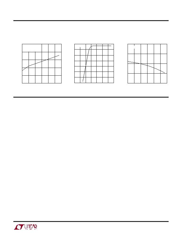
Typical perForMance characTerisTics
Gain Pin Voltage vs Temperature
V
GATE
vs V
CC
V
GATE
vs Temperature
pin FuncTions
UV (Pin 1): Undervoltage Pin. The threshold is set at 1.244V
with a 24mV hysteresis. When the UV pin is pulled high,
the charge pump ramps the GATE pin. When the UV pin
is pulled low, the GATE pin will be pulled low.
OV (Pin 2): Overvoltage Pin. The threshold is set at 1.220V
with a 15mV hysteresis. When the OV pin is pulled high,
the GATE pin is pulled low. After a timer cycle, the STATUS
pin is pulled low until the OV pin is pulled low.
TIMER (Pin 3): Analog System Timing Generator Pin.
This pin is used to set the delay before the load sharing
turns on after the UV pin goes high. The other use for
the TIMER pin is to delay the indication of a fault on the
STATUS pin.
When the timer is off, an internal N-channel shorts the
TIMER pin to ground. When the timer is turned on, a 2礎
or 6礎 timer current (I
TIMER
) from V
CC
is connected to the
TIMER pin and the voltage starts to ramp up with a slope
given by: dV/dt = I
TIMER
/C
T
. When the voltage reaches the
trip point (1.220V), the timer will be reset by pulling the
TIMER pin back to ground. The timer period is given by:
(1.220V " C
T
)/I
TIMER
.
GAIN (Pin 4): Analog Output Pin. The voltage across the
R
+
and R
pins is divided by a 1k resistor and sourced as
a current from the GAIN pin. An external resistor on the
GAIN pin determines the voltage gain from the current
sense resistor to the GAIN pin.
COMP2 (Pin 5): Analog Output Pin. This pin is the output
of the share bus error amplifier E/A2. (A compensation
capacitor between this pin and ground sets the crossover
frequency for the power supply adjustment loop.) In most
cases, this pin operates between 0.5V to 1.5V and repre-
sents a diode voltage up from the voltage at the R
SET
pin.
It is clamped at 3V . During start-up, this pin is clamped to
ground. After a timer cycle (and if the GATE pin is high),
the COMP2 pin is released.
COMP1 (Pin 6): Analog Output Pin. This pin is the output
of the voltage regulating error amplifier E/A1. A com-
pensation capacitor between this pin and ground sets
the crossover frequency of the share bus loop. This pin
operates a diode voltage up from the voltage at the SB
pin and is clamped at 8.4V .
SB (Pin 7): Analog Output Pin. This pin drives the share
bus used to communicate the value of shared load current
between several power supplies. There is an amplifier that
drives this pin a diode below the COMP1 pin using an internal
NPN as a pull-up and a 20k resistor as a pull-down.
TEMPERATURE (癈)
50
2.2
2.3
2.4
2.5
2.6
2.7
25
0
25
50
75
100
R
GAIN
= 25k
(V
R
+
V
R
) = 100mV
V
CC
= 5V
V
CC
(V)
0
10
11
13
6
10
9
8
2
4
8
12 14
7
6
12
T
A
= 25癈
TEMPERATURE (癈)
50
11.0
11.5
12.0
12.5
13.0
25
0
25
50
75
100
V
CC
= 5V
相關PDF資料 |
PDF描述 |
|---|---|
| MAX1299CEAE+ | IC TEMP SENS W/ADC 16-SSOP |
| MAX14544ETA+T | IC ACCY SWITCH OVP PROTECT 8TDFN |
| MAX1617AMEE+T | IC REMOTE/LOCAL TEMP SNSR 16QSOP |
| MAX1617MEE+T | IC REMOTE/LOCAL TEMP SNSR 16QSOP |
| MAX1619MEE+ | IC TEMP SENSOR W/ALARM 16-QSOP |
相關代理商/技術參數 |
參數描述 |
|---|---|
| LTC4352CDD#PBF | 功能描述:IC IDEAL DIODE CNTRL 12-DFN RoHS:是 類別:集成電路 (IC) >> PMIC - O 圈控制器 系列:- 標準包裝:1,000 系列:- 應用:電池備份,工業/汽車,大電流開關 FET 型:- 輸出數:5 內部開關:是 延遲時間 - 開啟:100ns 延遲時間 - 關閉:- 電源電壓:3 V ~ 5.5 V 電流 - 電源:250µA 工作溫度:0°C ~ 70°C 安裝類型:表面貼裝 封裝/外殼:16-SOIC(0.154",3.90mm 寬) 供應商設備封裝:16-SOIC N 包裝:帶卷 (TR) |
| LTC4352CDD#TRPBF | 功能描述:IC IDEAL DIODE CNTRL 12-DFN RoHS:是 類別:集成電路 (IC) >> PMIC - O 圈控制器 系列:- 標準包裝:1,000 系列:- 應用:電池備份,工業/汽車,大電流開關 FET 型:- 輸出數:5 內部開關:是 延遲時間 - 開啟:100ns 延遲時間 - 關閉:- 電源電壓:3 V ~ 5.5 V 電流 - 電源:250µA 工作溫度:0°C ~ 70°C 安裝類型:表面貼裝 封裝/外殼:16-SOIC(0.154",3.90mm 寬) 供應商設備封裝:16-SOIC N 包裝:帶卷 (TR) |
| LTC4352CMS#PBF | 功能描述:IC IDEAL DIODE CNTRL 12-MSOP RoHS:是 類別:集成電路 (IC) >> PMIC - O 圈控制器 系列:- 標準包裝:1,000 系列:- 應用:電池備份,工業/汽車,大電流開關 FET 型:- 輸出數:5 內部開關:是 延遲時間 - 開啟:100ns 延遲時間 - 關閉:- 電源電壓:3 V ~ 5.5 V 電流 - 電源:250µA 工作溫度:0°C ~ 70°C 安裝類型:表面貼裝 封裝/外殼:16-SOIC(0.154",3.90mm 寬) 供應商設備封裝:16-SOIC N 包裝:帶卷 (TR) |
| LTC4352CMS#TRPBF | 功能描述:IC IDEAL DIODE CNTRL 12-MSOP RoHS:是 類別:集成電路 (IC) >> PMIC - O 圈控制器 系列:- 標準包裝:1,000 系列:- 應用:電池備份,工業/汽車,大電流開關 FET 型:- 輸出數:5 內部開關:是 延遲時間 - 開啟:100ns 延遲時間 - 關閉:- 電源電壓:3 V ~ 5.5 V 電流 - 電源:250µA 工作溫度:0°C ~ 70°C 安裝類型:表面貼裝 封裝/外殼:16-SOIC(0.154",3.90mm 寬) 供應商設備封裝:16-SOIC N 包裝:帶卷 (TR) |
| LTC4352HDD#PBF | 功能描述:IC IDEAL DIODE CTLR W/MON 12-DFN RoHS:是 類別:集成電路 (IC) >> PMIC - O 圈控制器 系列:- 標準包裝:1,000 系列:- 應用:電池備份,工業/汽車,大電流開關 FET 型:- 輸出數:5 內部開關:是 延遲時間 - 開啟:100ns 延遲時間 - 關閉:- 電源電壓:3 V ~ 5.5 V 電流 - 電源:250µA 工作溫度:0°C ~ 70°C 安裝類型:表面貼裝 封裝/外殼:16-SOIC(0.154",3.90mm 寬) 供應商設備封裝:16-SOIC N 包裝:帶卷 (TR) |
發布緊急采購,3分鐘左右您將得到回復。