- 您現在的位置:買賣IC網 > PDF目錄370973 > M5M4V16169DTP (Mitsubishi Electric Corporation) 16MCDRAM:16M(1M-WORD BY 16-BIT) CACHED DRAM WITH 16K (1024-WORD BY 16-BIT) SRAM PDF資料下載
參數資料
| 型號: | M5M4V16169DTP |
| 廠商: | Mitsubishi Electric Corporation |
| 英文描述: | 16MCDRAM:16M(1M-WORD BY 16-BIT) CACHED DRAM WITH 16K (1024-WORD BY 16-BIT) SRAM |
| 中文描述: | 16MCDRAM:16米(100萬字由16位)與16K的緩存內存(1024字由16位)的SRAM |
| 文件頁數: | 1/64頁 |
| 文件大小: | 737K |
| 代理商: | M5M4V16169DTP |
當前第1頁第2頁第3頁第4頁第5頁第6頁第7頁第8頁第9頁第10頁第11頁第12頁第13頁第14頁第15頁第16頁第17頁第18頁第19頁第20頁第21頁第22頁第23頁第24頁第25頁第26頁第27頁第28頁第29頁第30頁第31頁第32頁第33頁第34頁第35頁第36頁第37頁第38頁第39頁第40頁第41頁第42頁第43頁第44頁第45頁第46頁第47頁第48頁第49頁第50頁第51頁第52頁第53頁第54頁第55頁第56頁第57頁第58頁第59頁第60頁第61頁第62頁第63頁第64頁
M5M4V16169DTP/RT-7,-8,-10,-15
16MCDRAM:16M(1M-WORD BY 16-BIT) CACHED DRAM WITH 16K (1024-WORD BY 16-BIT) SRAM
MITSUBISHI LSIs
(REV 1.0) Jul. 1998
MITSUBISHI ELECTRIC
1.
2.
Preliminary
This document is a preliminary Target Spec. and some of the contents are subject to change without notice.
# 70-pin,400-mil TSOP (type II ) with 0.65mm
lead pitch and 23.49mm package length.
# Multiplexed DRAM address inputs for reduced pin
count and higher system densities.
# Selectable output operation (transparent / latched /
registered) using set command register cycle.
# Single 3.3V +/- 0.3V Power Supply.
(3.3V +/- 0.15V for -7 part)
# 2048 refresh cycles every 64ms (Ad0->Ad10).
# Programmable burst length (1,2,4,8) and burst
sequence (sequential,interleave) with no latency.
# Synchronous design for precise control with
an external clock (K).
# Output retention by advanced mask clock (CMs#).
# All inputs/outputs low capacitance and LVTTL
compatible.
# Separate DRAM and SRAM address inputs
for fast SRAM access.
# Page Mode capability.
# Auto Refresh capability.
# Self Refresh capability.
: Master Clock
: Chip Select
: DRAM Clock Mask
: Row Addr. Strobe
: Column Addr. Strobe
: Data Transfer Direction
: DRAM Address
: SRAM Clock Mask
: Control Clocks
: Write Enable
: I/O Byte Control
: SRAM Address
: Output Enable
: Data I/O
: Power Supply
: DQ Power Supply
: Ground
:Address Fetch clock
This pin can be None-Connect.
:Must Connect Low
:Must Connect High
1
DESCRIPTION
The M5M4V16169DTP/RT is a 16M-bit Cached DRAM which integrates input
registers, a 1,048,576-word by 16-bit dynamic memory array and a 1024- word
by 16-bit static RAM array as a Cache memory (block size 8x16) onto a single
monolithic circuit. The block data transfer between the DRAM and the data
transfer buffers (RB1/RB2/WB1/WB2) is performed in one instruction cycle, a
fundamental advantage over a conventional DRAM/SRAM cache.
The RAM is fabricated with a high performance CMOS process, and is ideal for
large-capacity memory systems where high speed, low power dissipation, and
low cost are essential. The use of quadruple-layer polysilicon process combined
with silicide and double layer aluminum wiring technology, a single-transistor
dynamic storage stacked capacitor cell, and a six-transistor static storage cache
cell provide high circuit density at reduced costs.
22
23
24
25
26
27
28
29
30
31
32
33
34
35
14
15
16
17
7
8
9
10
11
12
13
19
20
21
1
2
3
4
5
6
49
48
47
46
45
44
43
42
41
40
39
38
37
36
57
56
55
54
64
63
62
61
60
59
58
52
51
50
70
69
68
67
66
65
Vss
DQ14
DQ9
Vss
DQ8
MCH
As4
As3
Ad6
Ad5
Ad4
Ad3
ADF#
Vss
DQ13
VccQ
DQ12
Vcc
As9
As8
As7
As6
DQ15
DQ11
VccQ
DQ10
G#
As5
Vss
Ad9
Ad8
Ad7
Ad11
Ad10
Vss
DQ7
MCL
Vss
DQ1
DQ6
As2
RAS#
CAS#
DTD#
Ad0
Ad1
Ad2
Vcc
DQ2
VddQ
DQ3
Vss
CS#
CMd#
CMs#
DQ4
VccQ
DQ5
As0
As1
Vcc
DQCl
DQCu
CC1#
CC0#
WE#
K
DQ0
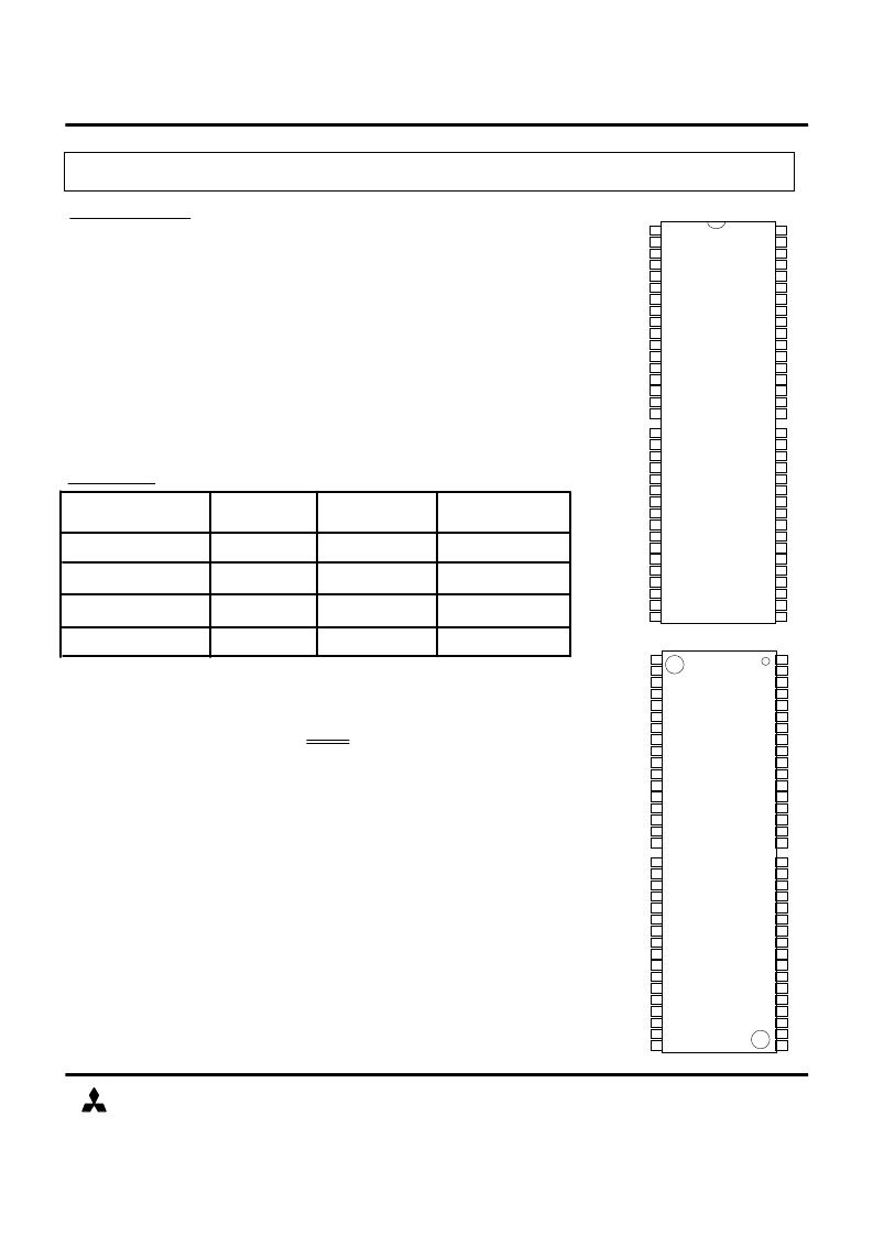
Package code:70P3S-L
400 mil
70Pin
TSOP
Type II
0.65mm
Lead
Pitch
FEATURES
Power
Dissipation (Typ)
SRAM
Access/cycle
DRAM
Access/cycle
8.0ns/15ns
75ns/120ns
Type name
56ns/80ns
M5M4V16169TP/RT-15
6.4ns/8ns
DRAM: 500
SRAM: 800
DRAM: 430
SRAM: 660
DRAM: 330
SRAM: 420
M5M4V16169TP/RT-8
M5M4V16169TP/RT-7
5.6ns/7ns
49ns/70ns
DRAM: 530
SRAM: 860
22
23
24
25
26
27
28
29
30
31
32
33
34
35
14
15
16
17
7
8
9
10
11
12
13
19
20
21
1
2
3
4
5
6
Vss
DQ7
MCL
Vss
DQ1
DQ6
As2
RAS#
CAS#
DTD#
Ad0
Ad1
Ad2
Vcc
DQ2
VccQ
DQ3
Vss
CS#
CMd#
CMs#
K
DQ0
DQ4
VccQ
DQ5
MCH
G#
As5
As0
As1
Vcc
DQCl
DQCu
CC1#
CC0#
WE#
Package code:70P3S-M
400 mil
70Pin
TSOP
Type II
0.65mm
Lead
Pitch
Vss
DQ9
Vss
DQ8
As4
As3
Ad6
Ad5
Ad4
Ad3
ADF#
Vss
DQ13
VccQ
DQ12
Vcc
As9
As8
As7
As6
DQ11
VccQ
DQ10
Vss
Ad9
Ad8
Ad7
Ad11
Ad10
DQ15
DQ14
49
48
47
46
45
44
43
42
41
40
39
38
37
36
57
56
55
54
64
63
62
61
60
59
58
52
51
50
70
69
68
67
66
65
PINCONFIGURATION
(TOP VIEW)
K
CS#
CMd#
RAS#
CAS#
DTD#
Ad
CMs#
CC0#,CC1#
WE#
DQC(u/l)
As
G#
DQ
Vcc
VccQ
Vss
ADF#
MCL
MCH
60ns/90ns
8.0ns/10ns
M5M4V16169TP/RT-10
相關PDF資料 |
PDF描述 |
|---|---|
| M5M4V16169DRT-10 | 16MCDRAM:16M(1M-WORD BY 16-BIT) CACHED DRAM WITH 16K (1024-WORD BY 16-BIT) SRAM |
| M5M4V16169DRT-15 | 16MCDRAM:16M(1M-WORD BY 16-BIT) CACHED DRAM WITH 16K (1024-WORD BY 16-BIT) SRAM |
| M5M4V16169DRT-7 | 16MCDRAM:16M(1M-WORD BY 16-BIT) CACHED DRAM WITH 16K (1024-WORD BY 16-BIT) SRAM |
| M5M4V16169DRT-8 | 22182053 |
| M5M4V16G50DFP-10 | 16M (2-BANK x 262144-WORD x 32-BIT) Synchronous Graphics RAM |
相關代理商/技術參數 |
參數描述 |
|---|---|
| M5M4V16169DTP-10 | 制造商:MITSUBISHI 制造商全稱:Mitsubishi Electric Semiconductor 功能描述:16MCDRAM:16M(1M-WORD BY 16-BIT) CACHED DRAM WITH 16K (1024-WORD BY 16-BIT) SRAM |
| M5M4V16169DTP-15 | 制造商:MITSUBISHI 制造商全稱:Mitsubishi Electric Semiconductor 功能描述:16MCDRAM:16M(1M-WORD BY 16-BIT) CACHED DRAM WITH 16K (1024-WORD BY 16-BIT) SRAM |
| M5M4V16169DTP-7 | 制造商:MITSUBISHI 制造商全稱:Mitsubishi Electric Semiconductor 功能描述:16MCDRAM:16M(1M-WORD BY 16-BIT) CACHED DRAM WITH 16K (1024-WORD BY 16-BIT) SRAM |
| M5M4V16169DTP-8 | 制造商:MITSUBISHI 制造商全稱:Mitsubishi Electric Semiconductor 功能描述:16MCDRAM:16M(1M-WORD BY 16-BIT) CACHED DRAM WITH 16K (1024-WORD BY 16-BIT) SRAM |
| M5M4V16G50DFP-10 | 制造商:MITSUBISHI 制造商全稱:Mitsubishi Electric Semiconductor 功能描述:16M (2-BANK x 262144-WORD x 32-BIT) Synchronous Graphics RAM |
發布緊急采購,3分鐘左右您將得到回復。