- 您現在的位置:買賣IC網 > PDF目錄370991 > M66221SP (Mitsubishi Electric Corporation) 256 x 9-BIT MAIL-BOX PDF資料下載
參數資料
| 型號: | M66221SP |
| 廠商: | Mitsubishi Electric Corporation |
| 英文描述: | 256 x 9-BIT MAIL-BOX |
| 中文描述: | 256 × 9位企業郵箱 |
| 文件頁數: | 1/11頁 |
| 文件大小: | 119K |
| 代理商: | M66221SP |
M66221SP/FP
2 9-BIT MAIL-BOX
×
9-BIT MAIL-BOX
256
1
DESCRIPTION
The M66221 is a mail box that incorporates a complete CMOS shared
memory cell of 256
×
9-bit configuration using high-performance silicon
gate CMOS process technology, and is equipped with two access
ports of A and B.
Access ports A and B are equipped with independent addresses CS,
WE and OE control pins and I/O pins to allow independent and
asynchronous read/write operations from/to shared memory
individually. This product also incorporates a port adjustment
arbitration function in address contention from both ports.
FEATURES
Memory configuration of 256
×
9 bits
High-speed access, address access time 40ns (typ.)
Complete asynchronous accessibility from ports A and B
Completely static operation
Built-in port arbitration function
Low power dissipation CMOS design
5V single power supply
Not Ready output pin is provided (open drain output)
TTL direct-coupled I/O
3-state output for I/O pins.
APPLICATION
Inter-MPU data transfer memory, buffer memory for image processing
system.
FUNCTION
The M66221 is a mail box most suitable for inter-MPU data transfer
which is used in a multiport mode. Provision of two pairs of addresses
and data buses in its shared memory cell of 256
×
9 bit configuration
allows independent and asynchronous read/write operations from/to
two access ports of A and B individually.
This allows access to shared memory as simple RAM when viewing
from one MPU. The concurrent accessibility to shared memory from
two MPUs provides remarkable improvement of a multiport mode
processor system in throughput.
The arbitration function incorporated in the chip decides the first-in
port to assign a higher priority to the access from one MPU, even if
two MPUs contend for selection of the same address in shared
memory from ports A and B. A Not Ready signal “L” is output to the
last-in port and invalidates any access from the other MPU.
As a write operation to memory, one of addresses A
0
to A
7
is specified.
The CS signal is set to “L” to place one of I/O pins in the input mode.
Also, the WE signal is set to “L”. Data at the I/O pin is thus written
into memory.
As a read operation, the WE signal is set to “H”. Both CS signal and
OE signal are set to “L” to place one of I/O pins in the output mode.
One of addresses A
0
to A
7
is specified. Data at the specified address
is output to the I/O pin.
When the CS signal is set to “H”, the chip enters a non-select state
which inhibits a read and write operation. At this time, the output is
placed in the floating state (high impedance state), thus allowing OR
tie with another chip. When the OE signal is set to “H”, the output
enters the floating state. In the I/O bus mode, setting the OE signal
to “H” at a write time avoids contention of I/O bus data. When the CS
signal is set to Vcc, the output enters the full stand-by state to minimize
supply current (See Tables 1 and 2).
MIMITSUBISHI
DIDIGITAL ASSP
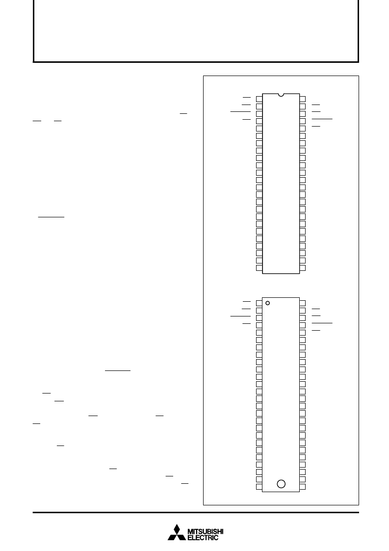
PIN CONFIGURATION (Top view)
CSA
→
→
←
→
→
→
→
→
→
→
→
→
I/O
0
B
←
←
←
←
←
←
←
←
←
→
←
←
1
2
25
48
47
46
45
WEA
Not Ready A
OEA
NC
I/O
7
A
I/O
8
A
GND
I/O
6
A
I/O
5
A
I/O
4
A
I/O
3
A
I/O
2
A
I/O
1
A
I/O
0
A
A
7
A
NC
A
6
A
A
5
A
A
4
A
A
3
A
A
2
A
A
1
A
A
0
A
CSB
WEB
V
CC
Not Ready B
OEB
OUTPUT ENABLE INPUT
NC
A
0
B
A
1
B
A
2
B
A
3
B
A
4
B
A
5
B
A
6
B
A
7
B
NC
I/O
7
B
I/O
6
B
I/O
5
B
I/O
4
B
I/O
3
B
I/O
2
B
I/O
1
B
CHIP SELECT INPUT
WRITE ENABLE INPUT
NOT READY
OUTPUT
OUTPUT ENABLE INPUT
A PORT
ADDRESS
INPUT
A PORT
DATA I/O
CHIP SELECT INPUT
WRITE ENABLE INPUT
NOT READY
OUTPUT
B PORT
ADDRESS
INPUT
B PORT
DATA I/O
Outline 48P4B
M
24
3
4
5
6
7
8
9
10
11
12
13
14
15
16
17
18
19
20
21
22
23
26
27
28
29
30
31
32
33
34
35
36
37
38
39
40
41
42
43
44
I/O
8
B
→
→
←
3
→
→
→
→
→
→
→
→
→
I/O
0
B
←
←
←
←
←
←
←
←
←
→
←
←
1
2
29
28
52
51
50
49
I/O
7
A
I/O
8
A
GND
I/O
6
A
I/O
5
A
I/O
4
A
I/O
3
A
I/O
2
A
I/O
1
A
I/O
0
A
A
7
A
NC
NC
A
6
A
A
5
A
A
4
A
A
3
A
A
2
A
A
1
A
A
0
A
A
0
B
A
1
B
A
2
B
A
3
B
A
4
B
A
5
B
A
6
B
A
7
B
NC
NC
I/O
7
B
I/O
6
B
I/O
5
B
I/O
4
B
I/O
3
B
I/O
2
B
I/O
1
B
Outline 52P2G-A
M
4
5
6
7
8
9
10
11
12
13
14
15
16
17
18
19
20
21
22
23
24
25
30
31
32
33
34
35
36
37
38
39
40
41
42
43
44
45
46
47
48
NC
NC
NC
I/O
8
B
27
26
NC
NC: No Connection
CSA
WEA
Not Ready A
OEA
CSB
WEB
V
CC
Not Ready B
OEB
OUTPUT ENABLE INPUT
CHIP SELECT INPUT
WRITE ENABLE INPUT
NOT READY
OUTPUT
OUTPUT ENABLE INPUT
A PORT
ADDRESS
INPUT
A PORT
DATA I/O
CHIP SELECT INPUT
WRITE ENABLE INPUT
NOT READY
OUTPUT
B PORT
ADDRESS
INPUT
B PORT
DATA I/O
相關PDF資料 |
PDF描述 |
|---|---|
| M66230FP | A2RT(ADVANCED ASYNCHRONOUS RECEIVER & TRANSMITTER) |
| M66230P | A2RT(ADVANCED ASYNCHRONOUS RECEIVER & TRANSMITTER) |
| M66235 | STANDARD CLOCK GENERATOR |
| M66235FP | STANDARD CLOCK GENERATOR |
| M66236 | STANDARD CLOCK GENERATOR |
相關代理商/技術參數 |
參數描述 |
|---|---|
| M66222FP | 制造商:MITSUBISHI 制造商全稱:Mitsubishi Electric Semiconductor 功能描述:128 x 8-BIT x 2 MAIL-BOX |
| M66222SP | 制造商:RENESAS 制造商全稱:Renesas Technology Corp 功能描述:128*8-BIT*2 MAIL-BOX |
| M66223FP | 制造商:RENESAS 制造商全稱:Renesas Technology Corp 功能描述:Mail Box That Incorporates a Complete CMOS Shared Memory Cell |
| M66230FP | 制造商:MITSUBISHI 制造商全稱:Mitsubishi Electric Semiconductor 功能描述:A2RT(ADVANCED ASYNCHRONOUS RECEIVER & TRANSMITTER) |
| M66230P | 制造商:MITSUBISHI 制造商全稱:Mitsubishi Electric Semiconductor 功能描述:A2RT(ADVANCED ASYNCHRONOUS RECEIVER & TRANSMITTER) |
發布緊急采購,3分鐘左右您將得到回復。