- 您現在的位置:買賣IC網 > Datasheet目錄43 > MAX5900AAEUT+T (Maxim Integrated)IC HOT-SWAP CONTROLLER SOT23-6 Datasheet資料下載
參數資料
| 型號: | MAX5900AAEUT+T |
| 廠商: | Maxim Integrated |
| 文件頁數: | 2/14頁 |
| 文件大小: | 290K |
| 描述: | IC HOT-SWAP CONTROLLER SOT23-6 |
| 產品培訓模塊: | Lead (SnPb) Finish for COTS Obsolescence Mitigation Program |
| 標準包裝: | 2,500 |
| 系列: | Simple Swapper™ |
| 類型: | 熱交換控制器 |
| 應用: | 通用 |
| 內部開關: | 無 |
| 電源電壓: | -9 V ~ -100 V |
| 工作溫度: | -40°C ~ 85°C |
| 安裝類型: | 表面貼裝 |
| 封裝/外殼: | SOT-23-6 |
| 供應商設備封裝: | SOT-6 |
| 包裝: | 帶卷 (TR) |
-100V, SOT23/TDFN, Simple Swapper
Hot-Swap Controllers
2 _______________________________________________________________________________________
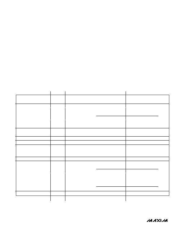
ABSOLUTE MAXIMUM RATINGS
ELECTRICAL CHARACTERISTICS
(V
EE
= -9V to -100V, GND = 0V, ON/OFF open circuit, T
A
= -40癈 to +85癈, unless otherwise noted. Typical values are at V
EE
= -48V
and T
A
= +25癈.) (Notes 1, 2)
Stresses beyond those listed under
Absolute Maximum Ratings
may cause permanent damage to the device. These are stress ratings only, and functional
operation of the device at these or any other conditions beyond those indicated in the operational sections of the specifications is not implied. Exposure to
absolute maximum rating conditions for extended periods may affect device reliability.
Terminal Voltage (with respect to GND, unless otherwise noted)
V
EE,
DRAIN, PGOOD, PGOOD ............................-120V to +0.3V
ON/OFF to V
EE
.........................................................-0.3V to +4V
GATE to V
EE
......................................................... -0.3V to +12V
Current into Any Pin............................................................?mA
Continuous Power Dissipation (T
A
= +70癈)
6-Pin SOT23 (derate 9.1mW/癈 above +70癈)...........727mW
6-Pin TDFN (derate 18.2mW/癈 above +70癈) ........1454mW
Junction to Case Thermal Resistance, ?/SPAN>
JC
(TDFN) ........8.5癈/W
Maximum Junction Temperature .....................................+150癈
Storage Temperature Range.............................-60癈 to +150癈
Lead Temperature (soldering, 10s).................................+300癈
PARAMETER
SYMBOL
CONDITIONS
MIN
TYP
MAX
UNITS
Supply Voltage
V
EE
-100
-9
V
Supply Current
I
GND
Measured at GND
0.5
1.3
mA
V
EE
= -36V to -72V
7.5
9.5
11.6
V
EE
= -100V
8
10
11.6
External Gate Drive
V
GS
V
GATE
- V
EE
V
EE
= -9V
6
7
V
Load Voltage Slew-Rate
Magnitude
SR
| dV
DRAIN
/dt |, C
LOAD
= 10礔, V
EE
= -9V to -36V
4.5
10
17
V m
Default UVLO
V
UVLO
|V
EE
| increasing
-34.5
-31.5
-28.5
V
UVLO Hysteresis
3.5
V
ON/OFF Input Resistance
R
ON/OFF
20
32
50
k&
Drain to V
EE
Resistance
R
DVEE
466
k&
ON/OFF Reference
Threshold
V
ON/OFF
(V
ON/OFF
- V
EE
) increasing
1.14
1.26
1.38
V
ON/OFF Hysteresis
140
mV
Start Delay (Note 3)
t
ON
150
300
500
ms
N FF ff D l
N
4
t
OFF
V
GATE
- V
EE
< 1V
9
20
32
ms
MAX590_ _AEUT
170
200
240
MAX590_ _BEUT
265
300
345
Circuit-Breaker
Threshold
V
CB
V
DRAIN
- V
EE
MAX590_ _CEUT
365
400
455
mV
C
GATE
= 1nF
1.5
3
C
GATE
= 4.7nF
2.5
4.5
Circuit-Breaker Delay
(Note 5)
t
CB
(V
DRAIN
- V
EE
) > V
CB
until (V
GATE
- V
EE
) <
1V, 200mV overdrive
step
C
GATE
= 10nF
4
6
祍
Restart Delay (Note 3)
t
RS
After circuit-breaker event, MAX590_A_EUT only
150
300
500
ms
相關PDF資料 |
PDF描述 |
|---|---|
| MAX5903LAETT+T | IC HOT-SWAP CONTROLLER 6-TDFN |
| MAX5909EEE+ | IC HOT-SWAP CTRLR DUAL 16QSOP |
| MAX5911ESA | IC SW HOTSWAP -48V SWAPPER 8SOIC |
| MAX5913AEMH+ | IC HOT SWAP CTLR QUAD 48V 44MQFP |
| MAX5916EUI+ | IC HOT-SWAP CTRLR DUAL 28-TSSOP |
相關代理商/技術參數 |
參數描述 |
|---|---|
| MAX5900ABETT | 制造商:Maxim Integrated Products 功能描述:SIMPLE SWAPPER HOT-SWAP CONTROLLER - Rail/Tube |
| MAX5900ABETT+ | 制造商:Maxim Integrated Products 功能描述:SIMPLE SWAPPER HOT-SWAP CONTROLLER - Rail/Tube |
| MAX5900ABETT+T | 功能描述:熱插拔功率分布 100V- Hot-Swap Controller RoHS:否 制造商:Texas Instruments 產品:Controllers & Switches 電流限制: 電源電壓-最大:7 V 電源電壓-最小:- 0.3 V 工作溫度范圍: 功率耗散: 安裝風格:SMD/SMT 封裝 / 箱體:MSOP-8 封裝:Tube |
| MAX5900ABETT-T | 功能描述:熱插拔功率分布 RoHS:否 制造商:Texas Instruments 產品:Controllers & Switches 電流限制: 電源電壓-最大:7 V 電源電壓-最小:- 0.3 V 工作溫度范圍: 功率耗散: 安裝風格:SMD/SMT 封裝 / 箱體:MSOP-8 封裝:Tube |
| MAX5900ABEUT | 制造商:Maxim Integrated Products 功能描述:SIMPLE SWAPPER HOT-SWAP CONTROLLER - Cut Tape Product |
發布緊急采購,3分鐘左右您將得到回復。