- 您現(xiàn)在的位置:買賣IC網(wǎng) > Datasheet目錄44 > MAX8563EEE+ (Maxim Integrated)IC REG CTRLR TRPL POS ADJ 16QSOP Datasheet資料下載
參數(shù)資料
| 型號: | MAX8563EEE+ |
| 廠商: | Maxim Integrated |
| 文件頁數(shù): | 11/15頁 |
| 文件大小: | 266K |
| 描述: | IC REG CTRLR TRPL POS ADJ 16QSOP |
| 產(chǎn)品培訓(xùn)模塊: | Lead (SnPb) Finish for COTS Obsolescence Mitigation Program |
| 標(biāo)準(zhǔn)包裝: | 100 |
| 類型: | 正,可調(diào)式 |
| 輸出數(shù): | 3 |
| 輸出電壓: | 0.5 V ~ 1.8 V,0.5 V ~ 3.3 V |
| 電流 - 電源: | 930µA |
| 輸入電壓: | 5V,12V |
| 工作溫度: | -40°C ~ 85°C |
| 封裝/外殼: | 16-SSOP(0.154",3.90mm 寬) |
| 供應(yīng)商設(shè)備封裝: | 16-QSOP |
| 包裝: | 管件 |
To set the output voltage to 0.5V, disconnect R
B
from
FB_ and connect it to OUT_; this change maintains the
minimum load requirement on the output. In this case,
R
A
can vary from 1k?to 10k?
Input and Output Capacitor Selection
The input filter capacitor aids in providing low input
impedance to the regulator and also reduces peak cur-
rents drawn from the power source during transient
conditions. Use a minimum 2.2礔 ceramic capacitor
from IN_ (drain of the external pass n-MOSFET) to GND
(see Figures 1 and 2). If large line transients or load
transients are expected, increase the input capaci-
tance to help minimize output voltage changes.
The output filter capacitor and its equivalent series
resistance (ESR) contribute to the stability of the regula-
tor (see the Stability Compensation section) and affect
the load-transient response. If large step loads (no load
to full load) are expected, and a very fast response
(less than a few microseconds) is required, use a
100礔, 18m?POSCAP for the output capacitor. If a
larger capacitance is desired, keep the capacitance
ESR product (C
OUT
x R
ESR
) in the 1祍 to 5祍 range.
If the application expects smaller load steps (less than
50% of full load), then use a 6.8礔 ceramic capacitor or
larger per ampere of maximum output current. This
option reduces the size and cost of the regulator circuit.
Note that some ceramic dielectrics exhibit large capaci-
tance variation with temperature. Use X7R or X5R
dielectrics to ensure sufficient capacitance at all operat-
ing temperatures. Tantalum and aluminum capacitors
are not recommended.
Power MOSFET Selection
The MAX8563/MAX8564/MAX8564A use an n-channel
MOSFET as the series pass transistor instead of a p-
channel MOSFET to reduce cost. The selected MOS-
FET must have a gate threshold voltage that meets the
following criteria:
V
GS_MAX
d V
DD
- V
OUT_
where V
DD
is the controller bias voltage, and V
GS_MAX
is the maximum gate voltage required to yield the on-
resistance (R
DS_ON
) specified by the manufacturers
data sheet. R
DS_ON
multiplied by the maximum output
current (load current) is the maximum voltage dropout
across the MOSFET, V
DS
_
MIN
. Make sure that V
DS
_
MIN
meets the condition below to avoid entering dropout,
where output voltage starts to decrease and any ripple
on the input also passes through to the output:
V
IN_MIN
> V
DS
_
MIN
+ V
OUT
where V
IN_MIN
is the minimum input voltage at the drain
of the MOSFET. V
DS
_
MIN
has a positive temperature
coefficient; therefore, the value of V
DS
_
MIN
at the highest
operating junction temperature should be used.
For thermal management, the maximum power dissipa-
tion in the MOSFET is calculated by:
P
D
= (V
IN_MAX
- V
OUT
) x I
OUT_MAX
The MOSFET is typically in an SMT package. Refer to
the MOSFET data sheet for the PC board area needed
to meet the maximum operating junction temperature
required.
Stability Compensation
Connect a resistor, R
C
, and a capacitor, C
C
, in series
from the DRV_ pin to GND. The values of the compen-
sation network depend upon the external MOSFET
characteristics, the output current range, and the pro-
grammed output voltage. The following parameters are
needed from the MOSFET data sheet: the input capaci-
tance (C
ISS
at V
DS
= 1V), the typical forward transcon-
ductance (g
FS
), and the current at which g
FS
was
measured (I
DFS
). Calculate the transconductance of
the FET at the maximum load current (I
OUT_MAX
):
g
g
I
I
C MAX
FS
OUT MAX
DFS
(
)
_
=
?/DIV>
R
V
V
R
V
A
B
OUT
FB
B
OUT
=
?/DIV>
?/DIV>
?/DIV>
?/DIV>
?/DIV>
?/DIV>
?/DIV>
?/DIV>
?/DIV>
?/DIV>
?/DIV>
?/DIV>
?/DIV>
主站蜘蛛池模板:
永宁县|
璧山县|
两当县|
监利县|
湖北省|
平顶山市|
墨玉县|
大姚县|
宁陕县|
襄垣县|
长子县|
紫阳县|
长寿区|
新化县|
平潭县|
南投县|
桐柏县|
永昌县|
玛曲县|
奉贤区|
会泽县|
锡林郭勒盟|
茂名市|
英吉沙县|
昌乐县|
广汉市|
柏乡县|
德化县|
栾川县|
江北区|
伊宁县|
且末县|
兴城市|
古田县|
阳西县|
宜黄县|
珲春市|
白河县|
平潭县|
福泉市|
安福县|
?/DIV>
?/DIV>
=
?/DIV>
?/DIV>
(
)
1
2
1
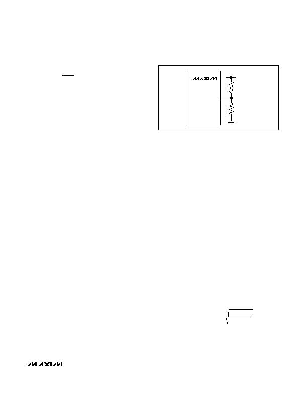
?%, Ultra-Low Output Voltage, Dual and Triple
Linear n-FET Controllers
______________________________________________________________________________________ 11
MAX8563
MAX8564
MAX8564A
FB_
OUT_
R
A
R
B
Figure 5. Adjustable Output Voltage
相關(guān)PDF資料 |
PDF描述 |
|---|---|
| MAX8667ETEAA+ | IC REG QD BCK/LINEAR SYNC 16TQFN |
| MAX8836ZEREEE+T | IC REG DL BCK/LINEAR SYNC 16UCSP |
| MAX8884YEREKE+T | IC REG TRPL BCK/LINEAR 16UCSP |
| MAX8896EREE+T | IC REG TRPL BCK/LINEAR 16UCSP |
| MC33232PG | IC PFC CONTROLLER CRM 8DIP |
相關(guān)代理商/技術(shù)參數(shù) |
參數(shù)描述 |
|---|---|
| MAX8563EEE+ | 功能描述:低壓差控制器 - LDO Dual & Triple Linear n-FET Controller RoHS:否 制造商:Micrel 最大輸入電壓:5.5 V 輸出電壓:Adjustable 輸出電流:10 mA 負(fù)載調(diào)節(jié): 輸出類型:Adjustable, Fixed 輸出端數(shù)量:1 最大工作溫度:+ 125 C 安裝風(fēng)格:SMD/SMT 封裝 / 箱體:SOT-23-6 |
| MAX8563EEE+T | 功能描述:低壓差控制器 - LDO Dual & Triple Linear n-FET Controller RoHS:否 制造商:Micrel 最大輸入電壓:5.5 V 輸出電壓:Adjustable 輸出電流:10 mA 負(fù)載調(diào)節(jié): 輸出類型:Adjustable, Fixed 輸出端數(shù)量:1 最大工作溫度:+ 125 C 安裝風(fēng)格:SMD/SMT 封裝 / 箱體:SOT-23-6 |
| MAX8563EEE-T | 功能描述:低壓差控制器 - LDO RoHS:否 制造商:Micrel 最大輸入電壓:5.5 V 輸出電壓:Adjustable 輸出電流:10 mA 負(fù)載調(diào)節(jié): 輸出類型:Adjustable, Fixed 輸出端數(shù)量:1 最大工作溫度:+ 125 C 安裝風(fēng)格:SMD/SMT 封裝 / 箱體:SOT-23-6 |
| MAX8564AEUB | 功能描述:低壓差穩(wěn)壓器 - LDO RoHS:否 制造商:Texas Instruments 最大輸入電壓:36 V 輸出電壓:1.4 V to 20.5 V 回動(dòng)電壓(最大值):307 mV 輸出電流:1 A 負(fù)載調(diào)節(jié):0.3 % 輸出端數(shù)量: 輸出類型:Fixed 最大工作溫度:+ 125 C 安裝風(fēng)格:SMD/SMT 封裝 / 箱體:VQFN-20 |
| MAX8564AEUB+ | 功能描述:低壓差控制器 - LDO Dual & Triple Linear n-FET Controller RoHS:否 制造商:Micrel 最大輸入電壓:5.5 V 輸出電壓:Adjustable 輸出電流:10 mA 負(fù)載調(diào)節(jié): 輸出類型:Adjustable, Fixed 輸出端數(shù)量:1 最大工作溫度:+ 125 C 安裝風(fēng)格:SMD/SMT 封裝 / 箱體:SOT-23-6 |
發(fā)布緊急采購,3分鐘左右您將得到回復(fù)。