- 您現在的位置:買賣IC網 > Datasheet目錄44 > MAX8836ZEREEE+T (Maxim Integrated)IC REG DL BCK/LINEAR SYNC 16UCSP Datasheet資料下載
參數資料
| 型號: | MAX8836ZEREEE+T |
| 廠商: | Maxim Integrated |
| 文件頁數: | 7/19頁 |
| 文件大小: | 414K |
| 描述: | IC REG DL BCK/LINEAR SYNC 16UCSP |
| 產品培訓模塊: | Lead (SnPb) Finish for COTS Obsolescence Mitigation Program |
| 標準包裝: | 2,500 |
| 拓撲: | 降壓(降壓)同步(1),線性(LDO)(1) |
| 功能: | 任何功能 |
| 輸出數: | 2 |
| 頻率 - 開關: | 1.6MHz |
| 電壓/電流 - 輸出 1: | 3.4V,1.2A |
| 電壓/電流 - 輸出 2: | 2.85V,200mA |
| 帶 LED 驅動器: | 無 |
| 帶監控器: | 無 |
| 帶序列發生器: | 無 |
| 電源電壓: | 2.7 V ~ 5.5 V |
| 工作溫度: | -40°C ~ 85°C |
| 安裝類型: | 表面貼裝 |
| 封裝/外殼: | 16-SSOP(0.154",3.90mm 寬) |
| 供應商設備封裝: | 16-QSOP |
| 包裝: | 帶卷 (TR) |
1.2A PWM Step-Down Converter in
2mm x 2mm WLP/UCSP for PA Power
_______________________________________________________________________________________ 7
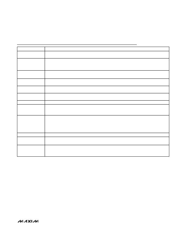
Pin Description
PIN NAME
FUNCTION
A1 REFBP
Reference Noise Bypass. Bypass REFBP to AGND with a 0.22礔 ceramic capacitor to reduce noise on the
LDO outputs. REFBP is internally pulled down through a 1k& resistor during shutdown.
A2 AGND
Low-Noise Analog Ground. Connect AGND to PGND using a common ground plane. Refer to the
MAX8805W Evaluation Kit for more information.
A3 N.I.C. Not Internally Connected. Connect to AGND for improved thermal performance.
A4 PGND
Power Ground for PA Step-Down Converter. Connect AGND to PGND using a common ground plane. Refer
to the MAX8805W Evaluation Kit for more information.
B1 LDO2
200mA LDO Regulator 2 Output. Bypass LDO2 with a 1礔 ceramic capacitor as close as possible to LDO2
and AGND. LDO2 is internally pulled down through a 1k& resistor when this regulator is disabled.
B2 PA_EN
PA Step-Down Converter Enable. Active-high enable input. Connect to IN1A/IN1B or logic-high for normal
operation. Pulled down to ground through an internal 800k& resistor.
B3
EN2
LDO2 Enable. Active-high enable input. Connect to IN2 or logic-high for normal operation. Pulled down to
ground through an internal 800k& resistor.
B4
LX Inductor Connection. Connect an inductor from LX to the output of the PA step-down converter.
C1
IN2
Supply Voltage Input for LDO2 and Internal Reference. Connect IN2 to a battery or supply voltage from
2.7V to 5.5V. Bypass IN2 with a 2.2礔 ceramic capacitor as close as possible to IN2 and AGND. Connect
IN2 to the same source as IN1A and IN1B.
C2
HP PA Output Voltage Select. Pulled down to ground through an internal 800k& resistor.
C3, C4
IN1B,
IN1A
Supply Voltage Input for PA Step-Down Converter. Connect IN1_ to a battery or supply voltage from 2.7V to
5.5V. Bypass the connection of IN1_ with a 4.7礔 ceramic capacitor as close as possible to IN1_ and
PGND. IN1A
and IN1B are internally connected together. Connect IN1_ to the same source as IN2.
D1
N.C. Internally Connected to IN2. Do not connect to this pin.
D2
T.P.
Test Point. This pin is used internally for factory test. This pin must be either externally connected to AGND
or unconnected. This pin has an internal 120k& pulldown to AGND.
D3, D4 PAB, PAA
PA Connection for Bypass Mode. Internally connected to IN1_ using the internal bypass MOSFET during
bypass mode. PA_ is connected to the internal feedback network. Bypass PA_ with a 4.7礔 ceramic
capacitor as close as possible to PA_ and PGND.
相關PDF資料 |
PDF描述 |
|---|---|
| MAX8884YEREKE+T | IC REG TRPL BCK/LINEAR 16UCSP |
| MAX8896EREE+T | IC REG TRPL BCK/LINEAR 16UCSP |
| MC33232PG | IC PFC CONTROLLER CRM 8DIP |
| MC33260DR2G | IC PFC CONTROLLER DCM 8SOIC |
| MC33262DG | IC PFC CONTROLLER CRM 8SOIC |
相關代理商/技術參數 |
參數描述 |
|---|---|
| MAX8836ZEWEEE+ | 制造商:Rochester Electronics LLC 功能描述: 制造商:Maxim Integrated Products 功能描述: |
| MAX8836ZEWEEE+T | 制造商:Maxim Integrated Products 功能描述: |
| MAX883C/D | 功能描述:低壓差穩壓器 - LDO RoHS:否 制造商:Texas Instruments 最大輸入電壓:36 V 輸出電壓:1.4 V to 20.5 V 回動電壓(最大值):307 mV 輸出電流:1 A 負載調節:0.3 % 輸出端數量: 輸出類型:Fixed 最大工作溫度:+ 125 C 安裝風格:SMD/SMT 封裝 / 箱體:VQFN-20 |
| MAX883C/D DIE | 制造商:Maxim Integrated Products 功能描述: |
| MAX883CPA | 功能描述:低壓差穩壓器 - LDO 5/3.3/AdjV 200mA Linear Regulator RoHS:否 制造商:Texas Instruments 最大輸入電壓:36 V 輸出電壓:1.4 V to 20.5 V 回動電壓(最大值):307 mV 輸出電流:1 A 負載調節:0.3 % 輸出端數量: 輸出類型:Fixed 最大工作溫度:+ 125 C 安裝風格:SMD/SMT 封裝 / 箱體:VQFN-20 |
發布緊急采購,3分鐘左右您將得到回復。