欧美成人免费电影,国产欧美一区二区三区精品酒店,精品国产a毛片,色网在线免费观看
- 您現在的位置:買賣IC網 > PDF目錄16784 > MAX9814EVKIT+ (Maxim Integrated Products)EVALUATION KIT FOR MAX9814 PDF資料下載
參數資料
| 型號: | MAX9814EVKIT+ |
| 廠商: | Maxim Integrated Products |
| 文件頁數: | 7/14頁 |
| 文件大小: | 0K |
| 描述: | EVALUATION KIT FOR MAX9814 |
| 產品培訓模塊: | Lead (SnPb) Finish for COTS Obsolescence Mitigation Program |
| 標準包裝: | 1 |
| 放大器類型: | AB 類 |
| 輸出類型: | 1-通道(單聲道) |
| 電源電壓: | 2.7V ~ 5.5V |
| 工作溫度: | -40°C ~ 85°C |
| 板類型: | 完全填充 |
| 已用 IC / 零件: | MAX9814 |
| 已供物品: | 板 |
Microphone Amplifier with AGC and
Low-Noise Microphone Bias
ABSOLUTE MAXIMUM RATINGS
ELECTRICAL CHARACTERISTICS
(VDD = 3.3V, SHDN = VDD, CCT = 470nF, CCG = 2F, GAIN = VDD, TA = TMIN to TMAX, unless otherwise specified. Typical values are
at TA = +25°C.) (Note 1)
Stresses beyond those listed under “Absolute Maximum Ratings” may cause permanent damage to the device. These are stress ratings only, and functional
operation of the device at these or any other conditions beyond those indicated in the operational sections of the specifications is not implied. Exposure to
absolute maximum rating conditions for extended periods may affect device reliability.
VDD to GND ..............................................................-0.3V to +6V
All Other Pins to GND.................................-0.3V to (VDD + 0.3V)
Output Short-Circuit Duration.....................................Continuous
Continuous Current (MICOUT, MICBIAS).......................±100mA
All Other Pins ....................................................................±20mA
Continuous Power Dissipation (TA = +70°C)
14-Pin TDFN-EP
(derate 16.7mW/°C above +70°C) ........................1481.5mW
Operating Temperature Range ...........................-40°C to +85°C
Junction Temperature ......................................................+150°C
Lead Temperature (soldering, 10s) .................................+300°C
Bump Temperature (soldering) Reflow............................+235°C
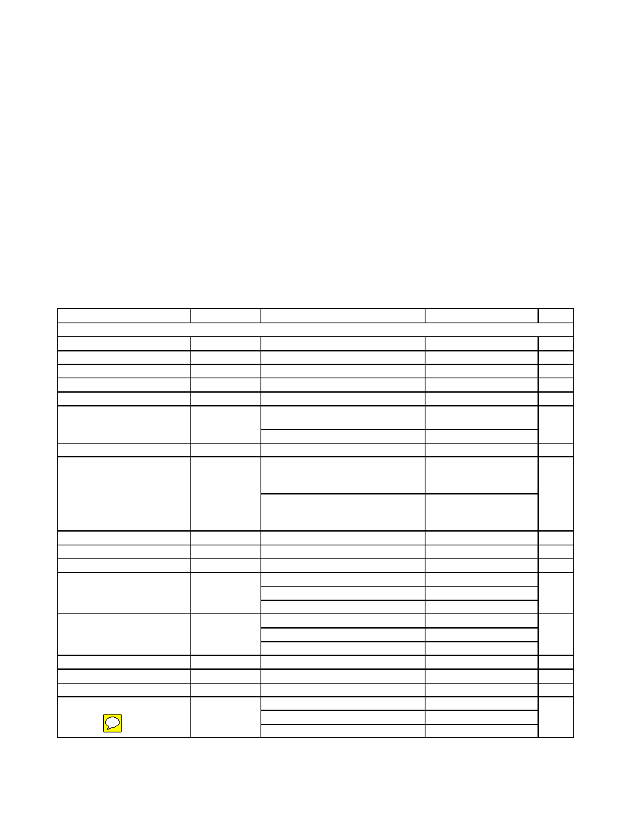
PARAMETER
SYMBOL
CONDITIONS
MIN
TYP
MAX
UNITS
GENERAL
Operating Voltage
VDD
Guaranteed by PSRR test
2.7
5.5
V
Supply Current
IDD
3.1
6
mA
Shutdown Supply Current
ISHDN
0.01
1
A
Input-Referred Noise Density
en
BW = 20kHz, all gain settings
30
nV/
√Hz
Output Noise
BW = 20kHz
430
VRMS
BW = 22Hz to 22kHz
(500mVRMS output signal)
61
Signal-to-Noise Ratio
SNR
A-weighted
64
dB
Dynamic Range
DR
(Note 2)
60
dB
fIN = 1kHz, BW = 20Hz to 20kHz,
RL = 10k
Ω, VTH = 1V (threshold = 2VP-P),
VIN = 0.5mVRMS, VCT = 0V
0.04
Total Harmonic Distortion Plus
Noise
THD+N
fIN = 1kHz, BW = 20Hz to 20kHz,
RL = 10k
Ω, VTH = 0.1V (threshold =
200mVP-P), VIN = 30mVRMS, VCT = 2V
0.2
%
Amplifier Input BIAS
VIN
1.14
1.23
1.32
V
Maximum Input Voltage
VIN_MAX
1% THD
100
mVP-P
Input Impedance
ZIN
100
k
Ω
GAIN = VDD
39.5
40
40.5
GAIN = GND
49.5
50
50.6
Maximum Gain
A
GAIN = unconnected
59.5
60
60.5
dB
GAIN = VDD
18.7
20
20.5
GAIN = GND
29.0
30
30.8
Minimum Gain
GAIN = unconnected
38.7
40
40.5
dB
Maximum Output Level
VOUT_RMS
1% THD+N, VTH = MICBIAS
0.707
VRMS
Regulated Output Level
AGC enabled, VTH = 0.7V
1.26
1.40
1.54
VP-P
AGC Attack Time
tATTACK
CCT = 470nF (Note 3)
1.1
ms
A/R = GND
1:500
A/R = VDD
1:2000
Attack/Release Ratio
A/R
A/R = unconnected
1:4000
ms/ms
MAX9814
2
Maxim Integrated
相關PDF資料 |
PDF描述 |
|---|---|
| H2MXH-3036G | DIP CABLE - HDM30H/AE30G/X |
| H3CCH-1606M | IDC CABLE - HKC16H/AE16M/HKC16H |
| 382A046-3-0 | BOOT MOLDED |
| V300C15T75BG | CONVERTER MOD DC/DC 15V 75W |
| MAX9789AEVKIT+ | EVALUATION KIT FOR MAX9789A |
相關代理商/技術參數 |
參數描述 |
|---|---|
| MAX9814EVKIT+ | 功能描述:音頻 IC 開發工具 MAX9814 Eval Kit RoHS:否 制造商:Texas Instruments 產品:Evaluation Kits 類型:Audio Amplifiers 工具用于評估:TAS5614L 工作電源電壓:12 V to 38 V |
| MAX981CPA | 功能描述:校驗器 IC Single Comparator / Reference RoHS:否 制造商:STMicroelectronics 產品: 比較器類型: 通道數量: 輸出類型:Push-Pull 電源電壓-最大:5.5 V 電源電壓-最小:1.1 V 補償電壓(最大值):6 mV 電源電流(最大值):1350 nA 響應時間: 最大工作溫度:+ 125 C 安裝風格:SMD/SMT 封裝 / 箱體:SC-70-5 封裝:Reel |
| MAX981CPA+ | 功能描述:校驗器 IC Single Comparator / Reference RoHS:否 制造商:STMicroelectronics 產品: 比較器類型: 通道數量: 輸出類型:Push-Pull 電源電壓-最大:5.5 V 電源電壓-最小:1.1 V 補償電壓(最大值):6 mV 電源電流(最大值):1350 nA 響應時間: 最大工作溫度:+ 125 C 安裝風格:SMD/SMT 封裝 / 箱體:SC-70-5 封裝:Reel |
| MAX981CSA | 功能描述:校驗器 IC RoHS:否 制造商:STMicroelectronics 產品: 比較器類型: 通道數量: 輸出類型:Push-Pull 電源電壓-最大:5.5 V 電源電壓-最小:1.1 V 補償電壓(最大值):6 mV 電源電流(最大值):1350 nA 響應時間: 最大工作溫度:+ 125 C 安裝風格:SMD/SMT 封裝 / 箱體:SC-70-5 封裝:Reel |
| MAX981CSA+ | 功能描述:校驗器 IC Single Comparator / Reference RoHS:否 制造商:STMicroelectronics 產品: 比較器類型: 通道數量: 輸出類型:Push-Pull 電源電壓-最大:5.5 V 電源電壓-最小:1.1 V 補償電壓(最大值):6 mV 電源電流(最大值):1350 nA 響應時間: 最大工作溫度:+ 125 C 安裝風格:SMD/SMT 封裝 / 箱體:SC-70-5 封裝:Reel |
發布緊急采購,3分鐘左右您將得到回復。