- 您現(xiàn)在的位置:買賣IC網(wǎng) > PDF目錄382289 > MBR0520LTI (National Semiconductor Corporation) DB-LM3S102 Daughterboard PDF資料下載
參數(shù)資料
| 型號: | MBR0520LTI |
| 廠商: | National Semiconductor Corporation |
| 英文描述: | DB-LM3S102 Daughterboard |
| 中文描述: | 同步降壓控制器,帶有預偏置啟動和可選時鐘同步 |
| 文件頁數(shù): | 17/23頁 |
| 文件大小: | 1002K |
| 代理商: | MBR0520LTI |
Application Information
(Continued)
as high as possible. Two zeroes f
and f
are placed at the
double pole frequency to cancel the double pole phase lag.
Then, a pole, f
P1
is placed at the frequency of the ESR zero.
A final pole f
is placed at one-half of the switching fre-
quency. The gain of the error amplifier transfer function is
selected to give the best bandwidth possible without violat-
ing the Nyquist stability criteria. In practice, a good crossover
point is one-fifth of the switching frequency, or 60 kHz for this
example. The generic equation for the error amplifier transfer
function is:
In this equation the variableA
is a ratio of the values of the
capacitance and resistance of the compensation compo-
nents, arranged as shown in
Figure 13
. A
is selected to
provide the desired bandwidth. A starting value of 80,000 for
A
should give a conservative bandwidth. Increasing the
value will increase the bandwidth, but will also decrease
phase margin. Designs with 45-60 are usually best because
they represent a good trade-off between bandwidth and
phase margin. In general, phase margin is lowest and gain
highest (worst-case) for maximum input voltage and mini-
mum output current. One method to select A
EA
is to use an
iterative process beginning with these worst-case conditions.
1.
Increase A
EA
2.
Check overall bandwidth and phase margin
3.
Change V
IN
to minimum and recheck overall bandwidth
and phase margin
4.
Change I
O
to maximum and recheck overall bandwidth
and phase margin
The process ends when the both bandwidth and the phase
margin are sufficiently high. For this example input voltage
can vary from 3.0 to 3.6V and output current can vary from 0
to 4A, and after a few iterations a moderate gain factor of
101dB is used.
The error amplifier of the LM2747 has a unity-gain band-
width of 9 MHz. In order to model the effect of this limitation,
the open-loop gain can be calculated as:
The new error amplifier transfer function that takes into
account unity-gain bandwidth is:
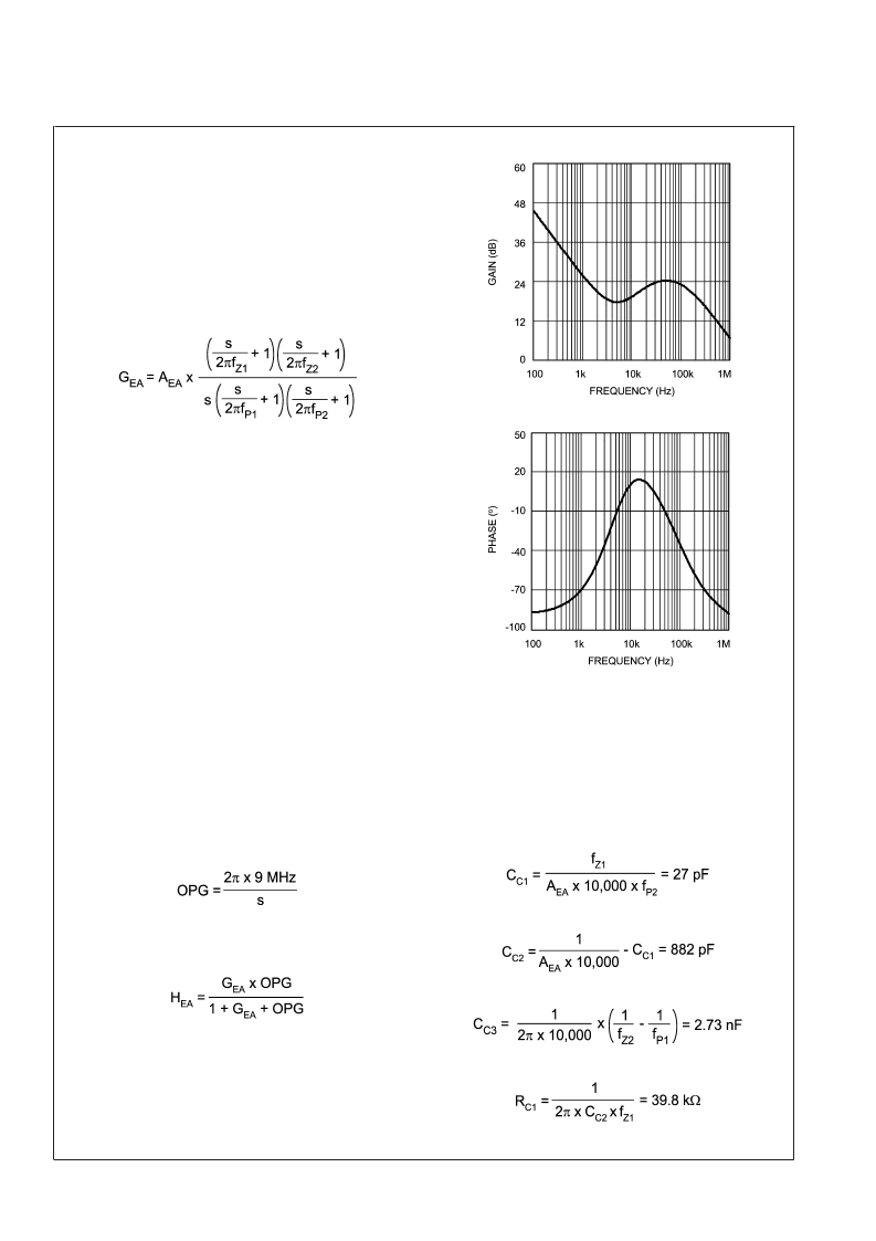
The gain and phase of the error amplifier are shown in
Figure 15
.
In VM regulators, the top feedback resistor R
FB2
forms a part
of the compensation. Setting R
to 10 k
±
1%, usually
gives values for the other compensation resistors and ca-
pacitors that fall within a reasonable range. (Capacitances
>
1 pF, resistances
<
1 M
) C
, C
, C
, R
, and R
are
selected to provide the poles and zeroes at the desired
frequencies, using the following equations:
20150974
20150975
FIGURE 15. Error Amp. Gain and Phase
L
www.national.com
17
相關PDF資料 |
PDF描述 |
|---|---|
| MBR1100 | SCHOTTKY BARRIER RECTIFIER 1.0 AMPERE 100 VOLTS |
| MBR1100RL | SCHOTTKY BARRIER RECTIFIER 1.0 AMPERE 100 VOLTS |
| MBR130LSFT1 | Surface Mount Schottky Power Rectifier Plastic SOD−123 Package |
| MBR130 | SCHOTTKY BARRIER RECTIFIER 1.0 AMPERES 30 VOLTS |
| MBR130T1 | SCHOTTKY BARRIER RECTIFIER 1.0 AMPERES 30 VOLTS |
相關代理商/技術參數(shù) |
參數(shù)描述 |
|---|---|
| MBR0520LTJ | 制造商:ARC-TRONICS 功能描述: |
| MBR0520L-TP | 功能描述:DIODE SCHOTTKY 0.5A 20V SOD-123 RoHS:是 類別:分離式半導體產(chǎn)品 >> 單二極管/整流器 系列:- 標準包裝:100 系列:- 二極管類型:標準 電壓 - (Vr)(最大):50V 電流 - 平均整流 (Io):6A 電壓 - 在 If 時為正向 (Vf)(最大):1.4V @ 6A 速度:快速恢復 = 200mA(Io) 反向恢復時間(trr):300ns 電流 - 在 Vr 時反向漏電:15µA @ 50V 電容@ Vr, F:- 安裝類型:底座,接線柱安裝 封裝/外殼:DO-203AA,DO-4,接線柱 供應商設備封裝:DO-203AA 包裝:散裝 其它名稱:*1N3879 |
| MBR0520LW | 制造商:KEXIN 制造商全稱:Guangdong Kexin Industrial Co.,Ltd 功能描述:Schottky Rectifier Diodes |
| MBR0520-M | 制造商:FORMOSA 制造商全稱:Formosa MS 功能描述:Chip Schottky Barrier Diodes - Silicon epitaxial planer type |
| MBR0520-N | 制造商:FORMOSA 制造商全稱:Formosa MS 功能描述:Chip Schottky Barrier Diodes - Silicon epitaxial planer type |
發(fā)布緊急采購,3分鐘左右您將得到回復。