參數資料
| 型號: | MC100EP196FAR2 |
| 廠商: | ON Semiconductor |
| 文件頁數: | 1/18頁 |
| 文件大小: | 0K |
| 描述: | IC DELAY LINE 1024TAP 32-LQFP |
| 標準包裝: | 1 |
| 系列: | 100EP |
| 標片/步級數: | 1024 |
| 功能: | 可編程 |
| 延遲到第一抽頭: | 2.36ns |
| 接頭增量: | 10ps |
| 可用的總延遲: | 2.36ns ~ 12.258ns |
| 獨立延遲數: | 1 |
| 電源電壓: | 3 V ~ 3.6 V |
| 工作溫度: | -40°C ~ 85°C |
| 安裝類型: | 表面貼裝 |
| 封裝/外殼: | 32-LQFP |
| 供應商設備封裝: | 32-LQFP(7x7) |
| 包裝: | 剪切帶 (CT) |
| 其它名稱: | MC100EP196FAROSCT |
Semiconductor Components Industries, LLC,2010
August, 2010 Rev. 15
1
Publication Order Number:
MC100EP196/D
MC100EP196
3.3VECL Programmable
Delay Chip with FTUNE
The MC100EP196 is a programmable delay chip (PDC) designed
primarily for clock deskewing and timing adjustment. It provides variable
delay of a differential NECL/PECL input transition. It has similar
architecture to the EP195 with the added feature of further tuneability in
delay using the FTUNE pin. The FTUNE input takes an analog voltage
from VCC to VEE to fine tune the output delay from 0 to 60 ps.
The delay section consists of a programmable matrix of gates and
multiplexers as shown in the logic diagram, Figure 2. The delay increment
of the EP196 has a digitally selectable resolution of about 10 ps and a net
range of up to 10.2 ns. The required delay is selected by the 10 data select
inputs D[9:0] values and controlled by the LEN (pin 10). A LOW level on
LEN allows a transparent LOAD mode of real time delay values by
D[9:0]. A LOW to HIGH transition on LEN will LOCK and HOLD
current values present against any subsequent changes in D[10:0]. The
approximate delay values for varying tap numbers correlating to D0 (LSB)
through D9 (MSB) are shown in Table 5.
Because the EP196 is designed using a chain of multiplexers, it has a
fixed minimum delay of 2.4 ns. An additional pin, D10, is provided for
controlling Pins 14 and 15, CASCADE and CASCADE, also latched
by LEN, in cascading multiple PDCs for increased programmable
range. The cascade logic allows full control of multiple PDCs.
Switching devices from all “1” states on D[0:9] with SETMAX LOW
to all “0” states on D[0:9] with SETMAX HIGH will increase the
delay equivalent to “D0”, the minimum increment.
Select input pins, D[10:0], may be threshold controlled by
combinations of interconnects between VEF (pin 7) and VCF (pin 8)
for LVCMOS, ECL, or LVTTL level signals. LVTTL and LVCMOS
operation is available in PECL mode only. For LVCMOS input levels,
leave VCF and VEF open. For ECL operation, short VCF and VEF
(pins 7 and 8). For LVTTL level operation, connect a 1.5 V supply
reference to VCF and leave open VEF pin. The 1.5 V reference voltage
to VCF pin can be accomplished by placing a 2.2 kW resistor between
VCF and VEE for 3.3 V power supply.
The VBB pin, an internally generated voltage supply, is available to
this device only. For singleended input conditions, the unused
differential input is connected to VBB as a switching reference voltage.
VBB may also rebias AC coupled inputs. When used, decouple VBB
and VCC via a 0.01 mF capacitor and limit current sourcing or sinking
to 0.5 mA. When not used, VBB should be left open.
The 100 Series contains temperature compensation.
Maximum Frequency > 1.2 GHz Typical
Programmable Range: 0 ns to 10 ns
Delay Range: 2.4 ns to 12.4 ns
10 ps Increments
PECL Mode Operating Range:
VCC = 3.0 V to 3.6 V with VEE = 0 V
NECL Mode Operating Range:
VCC = 0 V with VEE = 3.0 V to 3.6 V
Open Input Default State
Safety Clamp on Inputs
A Logic High on the EN Pin Will Force Q to Logic
Low
D[10:0] Can Accept Either ECL, LVCMOS, or LVTTL
Inputs
VBB Output Reference Voltage
PbFree Packages are Available*
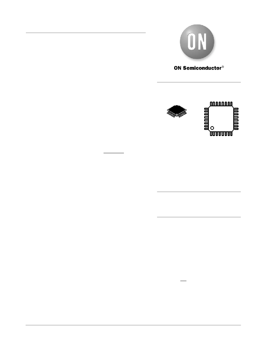
32
1
MC100
AWLYYWWG
EP196
LQFP32
FA SUFFIX
CASE 873A
MARKING
DIAGRAM*
A
= Assembly Location
WL
= Wafer Lot
YY
= Year
WW
= Work Week
G
= PbFree Package
*For additional marking information, refer to
Application Note AND8002/D.
http://onsemi.com
See detailed ordering and shipping information in the package
dimensions section on page 17 of this data sheet.
ORDERING INFORMATION
*For additional information on our PbFree strategy
and soldering details, please download the
ON Semiconductor Soldering and Mounting
Techniques Reference Manual, SOLDERRM/D.
相關PDF資料 |
PDF描述 |
|---|---|
| MC10E195FNR2 | IC DELAY LINE 128TAP 28-PLCC |
| MC10E196FNR2 | IC DELAY LINE 128TAP 28-PLCC |
| MC10EP195FAR2 | IC DELAY LINE 1024TAP 32-LQFP |
| MC10H640FNR2 | IC CLOCK DRIVER ECL-TTL 28-PLCC |
| MC10H642FNR2G | IC CLOCK DRIVER ECL-TTL 28-PLCC |
相關代理商/技術參數 |
參數描述 |
|---|---|
| MC100EP196FAR2G | 功能描述:延遲線/計時元素 3.3V/5V ECL Programmable Delay RoHS:否 制造商:Micrel 功能:Active Programmable Delay Line 傳播延遲時間:1000 ps 工作溫度范圍: 封裝 / 箱體:QFN-24 封裝:Tube |
| MC100EP210S | 制造商:ONSEMI 制造商全稱:ON Semiconductor 功能描述:2.5V1:5 Dual Differential LVDS Compatible Clock Driver |
| MC100EP210S_06 | 制造商:ONSEMI 制造商全稱:ON Semiconductor 功能描述:2.5V 1:5 Dual Differential LVDS Compatible Clock Driver |
| MC100EP210SFA | 功能描述:時鐘緩沖器 2.5V 1:5 Dual Diff RoHS:否 制造商:Texas Instruments 輸出端數量:5 最大輸入頻率:40 MHz 傳播延遲(最大值): 電源電壓-最大:3.45 V 電源電壓-最小:2.375 V 最大功率耗散: 最大工作溫度:+ 85 C 最小工作溫度:- 40 C 封裝 / 箱體:LLP-24 封裝:Reel |
| MC100EP210SFAG | 功能描述:時鐘緩沖器 2.5V 1:5 Dual Diff LVDS Clock Driver RoHS:否 制造商:Texas Instruments 輸出端數量:5 最大輸入頻率:40 MHz 傳播延遲(最大值): 電源電壓-最大:3.45 V 電源電壓-最小:2.375 V 最大功率耗散: 最大工作溫度:+ 85 C 最小工作溫度:- 40 C 封裝 / 箱體:LLP-24 封裝:Reel |
發布緊急采購,3分鐘左右您將得到回復。