- 您現在的位置:買賣IC網 > PDF目錄382290 > MC100EPT23DR2G (ON SEMICONDUCTOR) Dual Differential LVPECL to LVTTL Translator PDF資料下載
參數資料
| 型號: | MC100EPT23DR2G |
| 廠商: | ON SEMICONDUCTOR |
| 元件分類: | 通用總線功能 |
| 英文描述: | Dual Differential LVPECL to LVTTL Translator |
| 中文描述: | DUAL PECL TO TTL TRANSLATOR, TRUE OUTPUT, PDSO8 |
| 封裝: | LEAD FREE, SOIC-8 |
| 文件頁數: | 3/8頁 |
| 文件大小: | 65K |
| 代理商: | MC100EPT23DR2G |
MC100EPT23
http://onsemi.com
3
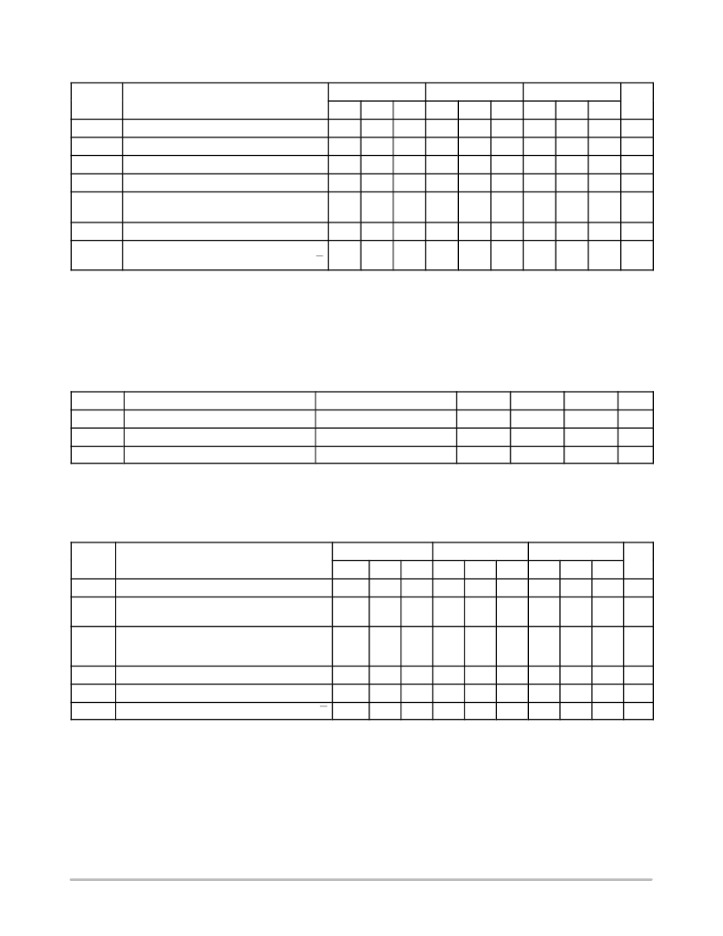
Table 4. PECL DC CHARACTERISTICS
V
CC
= 3.3 V, GND = 0 V (Note 2)
40
°
C
25
°
C
85
°
C
Symbol
Characteristic
Min
Typ
Max
Min
Typ
Max
Min
Typ
Max
Unit
I
CCH
Power Supply Current (Outputs set to HIGH)
10
18
25
10
18
25
10
18
25
mA
I
CCL
Power Supply Current (Outputs set to LOW)
15
26
36
15
26
36
15
26
36
mA
V
IH
Input HIGH Voltage
2075
2420
2075
2420
2075
2420
mV
V
IL
Input LOW Voltage
1355
1675
1355
1675
1355
1675
mV
V
IHCMR
Input HIGH Voltage Common Mode Range
(Note 3)
1.2
3.3
1.2
3.3
1.2
3.3
V
I
IH
Input HIGH Current
150
150
150
A
I
IL
Input LOW Current
D
D
150
150
150
150
150
150
0.5
A
NOTE: Device will meet the specifications after thermal equilibrium has been established when mounted in a test socket or printed circuit
board with maintained transverse airflow greater than 500 lfpm. Electrical parameters are guaranteed only over the declared
operating temperature range. Functional operation of the device exceeding these conditions is not implied. Device specification limit
values are applied individually under normal operating conditions and not valid simultaneously.
2. All values vary 1:1 with V
CC
.
3. V
IHCMR
min varies 1:1 with V
EE
, V
IHCMR
max varies 1:1 with V
CC
. The V
IHCMR
range is referenced to the most positive side of the differential
input signal.
Table 5. TTL DC CHARACTERISTICS
V
CC
= 3.3 V, GND = 0.0 V, T
A
= 40
°
C to 85
°
C
Symbol
Characteristic
Condition
Min
Typ
Max
Unit
V
OH
Output HIGH Voltage
I
OH
= 3.0 mA
2.4
V
V
OL
Output LOW Voltage
I
OL
= 24 mA
0.5
V
I
OS
Output Short Circuit Current
180
50
mA
NOTE: Device will meet the specifications after thermal equilibrium has been established when mounted in a test socket or printed circuit
board with maintained transverse airflow greater than 500 lfpm. Electrical parameters are guaranteed only over the declared
operating temperature range. Functional operation of the device exceeding these conditions is not implied. Device specification limit
values are applied individually under normal operating conditions and not valid simultaneously.
Table 6. AC CHARACTERISTICS
V
CC
= 3.0 V to 3.6 V, GND = 0.0 V
(Note 4)
40
°
C
25
°
C
85
°
C
Symbol
Characteristic
Min
Typ
Max
Min
Typ
Max
Min
Typ
Max
Unit
f
max
Maximum Frequency (Figure 2)
275
350
275
350
275
350
MHz
t
PLH
,
t
PHL
Propagation Delay to
Output Differential (Note 5)
1.2
1.2
1.5
1.5
1.8
1.8
1.2
1.1
1.5
1.5
1.8
1.8
1.3
1.1
1.7
1.5
2.4
1.8
ns
t
SK+ +
t
SK
t
SKPP
OutputtoOutput Skew++
OutputtoOutput Skew
ParttoPart Skew (Note 6)
15
35
70
60
80
500
15
40
70
70
80
500
30
40
140
125
80
500
ps
t
JITTER
Random Clock Jitter (RMS) (Figure 2)
5
10
5
10
5
10
ps
V
PP
Input Voltage Swing (Differential Configuration)
150
800
1200
150
800
1200
150
800
1200
mV
t
r
t
f
Output Rise/Fall Times (0.8 V 2.0 V)
Q, Q
330
600
900
330
600
900
330
650
900
ps
NOTE: Device will meet the specifications after thermal equilibrium has been established when mounted in a test socket or printed circuit
board with maintained transverse airflow greater than 500 lfpm. Electrical parameters are guaranteed only over the declared
operating temperature range. Functional operation of the device exceeding these conditions is not implied. Device specification limit
values are applied individually under normal operating conditions and not valid simultaneously.
4. Measured with a 750 mV 50% dutycycle clock source. R
L
= 500 to GND and C
L
= 20 pF to GND. Refer to Figure 3.
5. Reference (V
= 3.3V
±
5%; GND = 0 V)
6. Skews are measured between outputs under identical conditions.
相關PDF資料 |
PDF描述 |
|---|---|
| MC100EPT23D | Dual Differential LVPECL to LVTTL Translator |
| MC100EPT23DG | Dual Differential LVPECL to LVTTL Translator |
| MC100EPT23DT | Dual Differential LVPECL to LVTTL Translator |
| MC100EPT23DTG | Dual Differential LVPECL to LVTTL Translator |
| MC100EPT23DTR2 | Dual Differential LVPECL to LVTTL Translator |
相關代理商/技術參數 |
參數描述 |
|---|---|
| MC100EPT23DT | 功能描述:轉換 - 電壓電平 3.3V Dual Diff RoHS:否 制造商:Micrel 類型:CML/LVDS/LVPECL to LVCMOS/LVTTL 傳播延遲時間:1.9 ns 電源電流:14 mA 電源電壓-最大:3.6 V 電源電壓-最小:3 V 最大工作溫度:+ 85 C 安裝風格:SMD/SMT 封裝 / 箱體:MLF-8 |
| MC100EPT23DTG | 功能描述:轉換 - 電壓電平 3.3V Dual Diff LVPECL to LVTTL RoHS:否 制造商:Micrel 類型:CML/LVDS/LVPECL to LVCMOS/LVTTL 傳播延遲時間:1.9 ns 電源電流:14 mA 電源電壓-最大:3.6 V 電源電壓-最小:3 V 最大工作溫度:+ 85 C 安裝風格:SMD/SMT 封裝 / 箱體:MLF-8 |
| MC100EPT23DTG | 制造商:ON Semiconductor 功能描述:Translator / Logic Level Converter IC |
| MC100EPT23DTR2 | 功能描述:轉換 - 電壓電平 3.3V Dual Diff RoHS:否 制造商:Micrel 類型:CML/LVDS/LVPECL to LVCMOS/LVTTL 傳播延遲時間:1.9 ns 電源電流:14 mA 電源電壓-最大:3.6 V 電源電壓-最小:3 V 最大工作溫度:+ 85 C 安裝風格:SMD/SMT 封裝 / 箱體:MLF-8 |
| MC100EPT23DTR2G | 功能描述:轉換 - 電壓電平 3.3V Dual Diff LVPECL to LVTTL RoHS:否 制造商:Micrel 類型:CML/LVDS/LVPECL to LVCMOS/LVTTL 傳播延遲時間:1.9 ns 電源電流:14 mA 電源電壓-最大:3.6 V 電源電壓-最小:3 V 最大工作溫度:+ 85 C 安裝風格:SMD/SMT 封裝 / 箱體:MLF-8 |
發布緊急采購,3分鐘左右您將得到回復。