- 您現在的位置:買賣IC網 > PDF目錄369892 > MC10E336 (ON SEMICONDUCTOR) 3-BIT REGISTERED BUS TRANSCEIVER PDF資料下載
參數資料
| 型號: | MC10E336 |
| 廠商: | ON SEMICONDUCTOR |
| 英文描述: | 3-BIT REGISTERED BUS TRANSCEIVER |
| 中文描述: | 3位注冊總線收發器 |
| 文件頁數: | 1/4頁 |
| 文件大小: | 113K |
| 代理商: | MC10E336 |
SEMICONDUCTOR TECHNICAL DATA
2–1
REV 2
Motorola, Inc. 1996
12/93
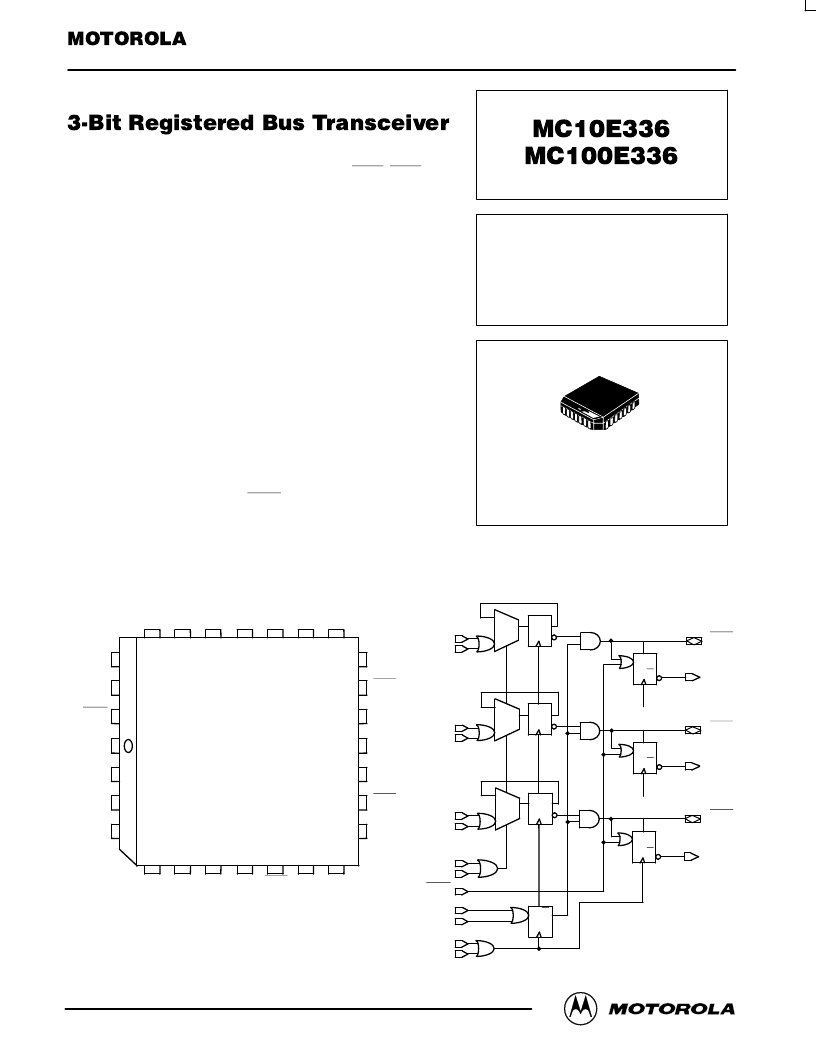
The MC10E/MC100E336 contains three bus transceivers with both
transmit and receive registers. The bus outputs (BUS0–BUS2) are
specified for driving a 25
bus; the receive outputs (Q0 – Q2) are
specified for 50
. The bus outputs feature a normal HIGH level (VOH) and
a cutoff LOW level — when LOW, the outputs go to –2.0V and the output
emitter-follower is “off”, presenting a high impedance to the bus. The bus
outputs also feature edge slow-down capacitors.
25
Cutoff Bus Outputs
50
Receiver Outputs
Transmit and Receive Registers
1500ps Max. Clock to Bus
1000ps Max. Clock to Q
Bus Outputs Feature Internal Edge Slow-Down Capacitors
Additional Package Ground Pins
Extended 100E VEE Range of – 4.2V to – 5.46V
75k
Input Pulldown Resistors
The Transmit Enable pins (TEN) control whether current data is held in
the transmit register, or new data is loaded from the A/B inputs. A LOW on
both of the Bus Enable inputs (BUSEN), when clocked through the
register, disables the bus outputs to –2.0V.
The receiver section clocks bus data into the receive registers, after
gating with the Receive Enable (RXEN) input.
All registers are clocked by a positive transition of CLK1 or CLK2 (or
both).
Additional leadframe grounding is provided through the Ground pins (GND) which should be connected to 0V. The GND pins
are not electrically connected to the chip.
LOGIC DIAGRAM
BUSEN1
BUSEN2
RXEN
VEE
CLK1
CLK2
A0
26
27
28
2
3
4
25
24
23
22
21
20
19
18
17
16
15
14
13
12
11
5
6
7
8
9
10
TEN2 TEN1
B2
A2
NC
VCCO
Q2
GND
BUS2
VCC
Q1
VCCO
BUS1
GND
B0
A1
B1
VCCOBUS0
GND
Q0
A0
B0
A1
B1
A2
B2
TEN1
TEN2
RXEN
BUSEN1
BUSEN2
CLK1
CLK2
D
D
D
D
D
D
D
Q
Q
Q
Q
Q
Q
Q
0
1
0
0
1
1
BUS0
BUS1
BUS2
50
50
50
25
CUTOFF
25
CUTOFF
25
CUTOFF
Q0
Q1
Q2
1
Pinout: 28-Lead PLCC
(Top View)
* All VCC and VCCO pins are tied together on the die.
3-BIT REGISTERED
BUS TRANSCEIVER
FN SUFFIX
PLASTIC PACKAGE
CASE 776-02
相關PDF資料 |
PDF描述 |
|---|---|
| MC10E336FN | 3-BIT REGISTERED BUS TRANSCEIVER |
| MC100E337FN | 3-BIT SCANNABLE REGISTERED BUS TRANSCEIVER |
| MC10E337 | Relays; Leaded Process Compatible:No; Peak Reflow Compatible (260 C):No; Features:SNAP OEM I/O Programmable Brain |
| MC10E337FN | 3-BIT SCANNABLE REGISTERED BUS TRANSCEIVER |
| MC100E431FN | 3-BIT DIFFERENTIAL FLIP-FLOP |
相關代理商/技術參數 |
參數描述 |
|---|---|
| MC10E404FI | 制造商:ON Semiconductor 功能描述: |
| MC10E404FN | 功能描述:邏輯門 5V ECL Quad Diff RoHS:否 制造商:Texas Instruments 產品:OR 邏輯系列:LVC 柵極數量:2 線路數量(輸入/輸出):2 / 1 高電平輸出電流:- 16 mA 低電平輸出電流:16 mA 傳播延遲時間:3.8 ns 電源電壓-最大:5.5 V 電源電壓-最小:1.65 V 最大工作溫度:+ 125 C 安裝風格:SMD/SMT 封裝 / 箱體:DCU-8 封裝:Reel |
| MC10E404FNG | 功能描述:邏輯門 5V ECL Quad Diff AND/NAND RoHS:否 制造商:Texas Instruments 產品:OR 邏輯系列:LVC 柵極數量:2 線路數量(輸入/輸出):2 / 1 高電平輸出電流:- 16 mA 低電平輸出電流:16 mA 傳播延遲時間:3.8 ns 電源電壓-最大:5.5 V 電源電壓-最小:1.65 V 最大工作溫度:+ 125 C 安裝風格:SMD/SMT 封裝 / 箱體:DCU-8 封裝:Reel |
| MC10E404FNR2 | 功能描述:邏輯門 5V ECL Quad Diff RoHS:否 制造商:Texas Instruments 產品:OR 邏輯系列:LVC 柵極數量:2 線路數量(輸入/輸出):2 / 1 高電平輸出電流:- 16 mA 低電平輸出電流:16 mA 傳播延遲時間:3.8 ns 電源電壓-最大:5.5 V 電源電壓-最小:1.65 V 最大工作溫度:+ 125 C 安裝風格:SMD/SMT 封裝 / 箱體:DCU-8 封裝:Reel |
| MC10E404FNR2G | 功能描述:邏輯門 5V ECL Quad Diff AND/NAND RoHS:否 制造商:Texas Instruments 產品:OR 邏輯系列:LVC 柵極數量:2 線路數量(輸入/輸出):2 / 1 高電平輸出電流:- 16 mA 低電平輸出電流:16 mA 傳播延遲時間:3.8 ns 電源電壓-最大:5.5 V 電源電壓-最小:1.65 V 最大工作溫度:+ 125 C 安裝風格:SMD/SMT 封裝 / 箱體:DCU-8 封裝:Reel |
發布緊急采購,3分鐘左右您將得到回復。