- 您現(xiàn)在的位置:買賣IC網(wǎng) > PDF目錄369896 > MC14027 (ON SEMICONDUCTOR) Dual J-K Flip-Flop PDF資料下載
參數(shù)資料
| 型號(hào): | MC14027 |
| 廠商: | ON SEMICONDUCTOR |
| 英文描述: | Dual J-K Flip-Flop |
| 中文描述: | 雙JK觸發(fā)器 |
| 文件頁數(shù): | 1/6頁 |
| 文件大小: | 213K |
| 代理商: | MC14027 |
MOTOROLA CMOS LOGIC DATA
Motorola, Inc. 1995
107
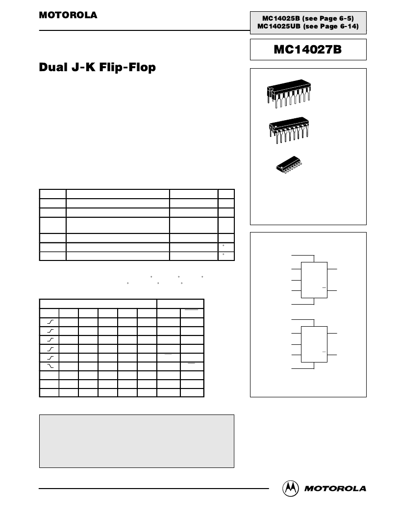
MC14027B
"
The MC14027B dual J–K flip–flop has independent J, K, Clock (C), Set (S)
and Reset (R) inputs for each flip–flop. These devices may be used in
control, register, or toggle functions.
Diode Protection on All Inputs
Supply Voltage Range = 3.0 Vdc to 18 Vdc
Logic Swing Independent of Fanout
Logic Edge–Clocked Flip–Flop Design —
Logic state is retained indefinitely with clock level either high or low;
information is transferred to the output only on the positive–going edge
of the clock pulse
Capable of Driving Two Low–power TTL Loads or One Low–power
Schottky TTL Load Over the Rated Temperature Range
(Voltages Referenced to VSS)
per Pin
Tstg
TL
* Maximum Ratings are those values beyond which damage to the device may occur.
Temperature Derating:
Plastic “P and D/DW” Packages: – 7.0 mW/ C From 65 C To 125 C
Ceramic “L” Packages: – 12 mW/ C From 100 C To 125 C
Power Dissipation, per Package
Storage Temperature
500
– 65 to + 150
mW
C
Lead Temperature (8–Second Soldering)
260
C
TRUTH TABLE
Inputs
Outputs*
C
J
K
S
R
Qn
0
Qn+1
1
Qn+1
0
1
X
0
0
X
0
0
0
1
1
0
0
X
0
0
0
0
1
X
1
0
0
1
0
1
1
1
0
0
Qo
Qo
Qo
X
X
0
0
X
Qn
1
Qn
0
X
X
X
1
0
X
X
X
X
0
1
X
0
1
X
X
X
1
1
X
1
1
X = Don’t Care
= Level Change
= Present State
* = Next State
This device contains protection circuitry to guard against damage
due to high static voltages or electric fields. However, precautions must
be taken to avoid applications of any voltage higher than maximum rated
voltages to this high-impedance circuit. For proper operation, Vin and
Vout should be constrained to the range VSS
≤
(Vin or Vout)
≤
VDD.
Unused inputs must always be tied to an appropriate logic voltage
level (e.g., either VSS or VDD). Unused outputs must be left open.
No
Change
SEMICONDUCTOR TECHNICAL DATA
REV 3
1/94
!
!
L SUFFIX
CERAMIC
CASE 620
ORDERING INFORMATION
MC14XXXBCP
MC14XXXBCL
MC14XXXBD
TA = – 55
°
to 125
°
C for all packages.
Plastic
Ceramic
SOIC
P SUFFIX
PLASTIC
CASE 648
D SUFFIX
SOIC
CASE 751B
BLOCK DIAGRAM
12
11
13
10
9
4
5
3
6
7
14
15
2
1
S
S
R
R
K
C
J
K
C
J
Q
Q
Q
Q
VDD = PIN 16
VSS = PIN 8
相關(guān)PDF資料 |
PDF描述 |
|---|---|
| MC14027BCP | Dual J-K Flip-Flop |
| MC14027BD | Dual J-K Flip-Flop |
| MC14027BDR2 | Dual-Slot Cardbus Power-Interface Switches for Serial PCMCIA Controllers 30-SSOP -40 to 85 |
| MC14027BF | Dual-Slot Cardbus Power-Interface Switches for Serial PCMCIA Controllers 30-SSOP -40 to 85 |
| MC14027B | Dual J-K Flip-Flop |
相關(guān)代理商/技術(shù)參數(shù) |
參數(shù)描述 |
|---|---|
| MC14027B | 制造商:MOTOROLA 制造商全稱:Motorola, Inc 功能描述:Dual J-K Flip-Flop |
| MC14027B_05 | 制造商:ONSEMI 制造商全稱:ON Semiconductor 功能描述:Dual J−K Flip−Flop |
| MC14027BCP | 功能描述:觸發(fā)器 3-18V CMOS Dual RoHS:否 制造商:Texas Instruments 電路數(shù)量:2 邏輯系列:SN74 邏輯類型:D-Type Flip-Flop 極性:Inverting, Non-Inverting 輸入類型:CMOS 輸出類型: 傳播延遲時(shí)間:4.4 ns 高電平輸出電流:- 16 mA 低電平輸出電流:16 mA 電源電壓-最大:5.5 V 最大工作溫度:+ 85 C 安裝風(fēng)格:SMD/SMT 封裝 / 箱體:X2SON-8 封裝:Reel |
| MC14027BCPG | 功能描述:觸發(fā)器 3-18V CMOS Dual JK-Type RoHS:否 制造商:Texas Instruments 電路數(shù)量:2 邏輯系列:SN74 邏輯類型:D-Type Flip-Flop 極性:Inverting, Non-Inverting 輸入類型:CMOS 輸出類型: 傳播延遲時(shí)間:4.4 ns 高電平輸出電流:- 16 mA 低電平輸出電流:16 mA 電源電壓-最大:5.5 V 最大工作溫度:+ 85 C 安裝風(fēng)格:SMD/SMT 封裝 / 箱體:X2SON-8 封裝:Reel |
| MC14027BD | 功能描述:觸發(fā)器 3-18V CMOS Dual RoHS:否 制造商:Texas Instruments 電路數(shù)量:2 邏輯系列:SN74 邏輯類型:D-Type Flip-Flop 極性:Inverting, Non-Inverting 輸入類型:CMOS 輸出類型: 傳播延遲時(shí)間:4.4 ns 高電平輸出電流:- 16 mA 低電平輸出電流:16 mA 電源電壓-最大:5.5 V 最大工作溫度:+ 85 C 安裝風(fēng)格:SMD/SMT 封裝 / 箱體:X2SON-8 封裝:Reel |
發(fā)布緊急采購,3分鐘左右您將得到回復(fù)。