參數資料
| 型號: | MC14528BFG |
| 廠商: | ON Semiconductor |
| 文件頁數: | 1/9頁 |
| 文件大小: | 0K |
| 描述: | IC MULTIVIBRATOR DUAL 16SOEIAJ |
| 產品變化通告: | 1Q2012 Discontinuation 30/Mar/2012 |
| 標準包裝: | 50 |
| 系列: | 4000B |
| 邏輯類型: | 單穩態 |
| 獨立電路: | 2 |
| 施密特觸發器輸入: | 無 |
| 傳輸延遲: | 90ns |
| 輸出電流高,低: | 8.8mA,8.8mA |
| 電源電壓: | 3 V ~ 18 V |
| 工作溫度: | -55°C ~ 125°C |
| 安裝類型: | 表面貼裝 |
| 封裝/外殼: | 16-SOIC(0.209",5.30mm 寬) |
| 供應商設備封裝: | 16-SOEIAJ |
| 包裝: | 管件 |
Semiconductor Components Industries, LLC, 2013
May, 2013 Rev. 8
1
Publication Order Number:
MC14528B/D
MC14528B
Dual Monostable
Multivibrator
The MC14528B is a dual, retriggerable, resettable monostable
multivibrator. It may be triggered from either edge of an input pulse,
and produces an output pulse over a wide range of widths, the duration
of which is determined by the external timing components,
CX and RX.
Features
Separate Reset Available
Diode Protection on All Inputs
Triggerable from Leading or Trailing Edge Pulse
Supply Voltage Range = 3.0 Vdc to 18 Vdc
Capable of Driving Two Lowpower TTL Loads or One Lowpower
Schottky TTL Load Over the Rated Temperature Range
This part should only be used in new designs where the pulse width
is < 10
ms
Note:
For designs requiring a pulse width > 10
ms, please see
MC14538, which is pinforpin compatible
These Devices are PbFree and are RoHS Compliant
NLV Prefix for Automotive and Other Applications Requiring
Unique Site and Control Change Requirements; AECQ100
Qualified and PPAP Capable
MAXIMUM RATINGS (Voltages Referenced to VSS)
Rating
Symbol
Value
Unit
DC Supply Voltage Range
VDD
0.5 to +18.0
V
Input or Output Voltage Range
(DC or Transient)
Vin, Vout
0.5 to VDD + 0.5
V
Input or Output Current
(DC or Transient) per Pin
Iin, Iout
±10
mA
Power Dissipation, per Package
(Note 1)
PD
500
mW
Ambient Temperature Range
TA
55 to +125
°C
Storage Temperature Range
Tstg
65 to +150
°C
Lead Temperature
(8Second Soldering)
TL
260
°C
Stresses exceeding Maximum Ratings may damage the device. Maximum
Ratings are stress ratings only. Functional operation above the Recommended
Operating Conditions is not implied. Extended exposure to stresses above the
Recommended Operating Conditions may affect device reliability.
1. Temperature Derating:
Plastic “P and D/DW” Packages: – 7.0 mW/_C From 65_C To 125_C
This device contains protection circuitry to guard against damage due to high
static voltages or electric fields. However, precautions must be taken to avoid
applications of any voltage higher than maximum rated voltages to this
highimpedance circuit. For proper operation, Vin and Vout should be constrained
to the range VSS v (Vin or Vout) v VDD.
Unused inputs must always be tied to an appropriate logic voltage level
(e.g., either VSS or VDD). Unused outputs must be left open.
http://onsemi.com
See detailed ordering and shipping information in the package
dimensions section on page 5 of this data sheet.
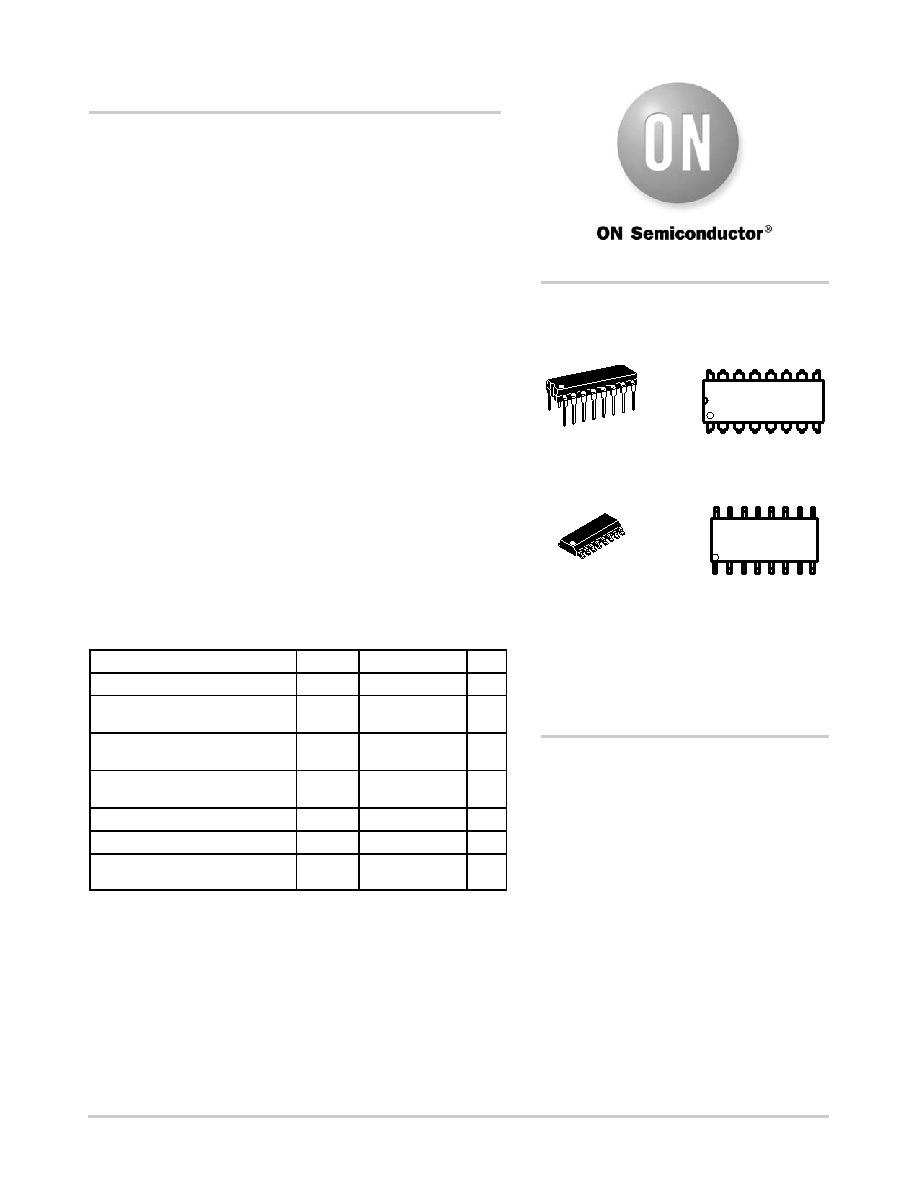
ORDERING INFORMATION
SOIC16
D SUFFIX
CASE 751B
MARKING
DIAGRAMS
14528BG
AWLYWW
PDIP16
P SUFFIX
CASE 648
1
MC14528BCP
AWLYYWWG
1
A
= Assembly Location
WL
= Wafer Lot
YY, Y
= Year
WW, W = Work Week
G
= PbFree Package
相關PDF資料 |
PDF描述 |
|---|---|
| MC14538BFEL | IC MULTIVIBRATOR DUAL 16SOEIAJ |
| MC14557BDWR2 | IC SHIFT REGISTER 1-64BIT 16SOIC |
| MC14559BCP | IC REGISTER 8BIT APPROX 16-DIP |
| MC14572UBDR2 | IC GATE HEX NAND/NOR/INV 16-SOIC |
| MC14584BFEL | IC SCHMITT TRIGGER HEX 14SOEIAJ |
相關代理商/技術參數 |
參數描述 |
|---|---|
| MC14528BFL2 | 制造商:Rochester Electronics LLC 功能描述:- Bulk |
| MC14528CP-D3-14528B-9 | 制造商:Harris Corporation 功能描述: |
| MC1452BCPG | 制造商:ON Semiconductor 功能描述: |
| MC14530BCP | 制造商:Motorola Inc 功能描述: |
| MC14531BCP | 制造商: 功能描述: 制造商:undefined 功能描述: |
發布緊急采購,3分鐘左右您將得到回復。