- 您現在的位置:買賣IC網 > PDF目錄385565 > MC14543BDR2 (ON SEMICONDUCTOR) BCD-to-Seven Segment Latch/Decoder/Driver for Liquid Crystals PDF資料下載
參數資料
| 型號: | MC14543BDR2 |
| 廠商: | ON SEMICONDUCTOR |
| 元件分類: | 通用總線功能 |
| 英文描述: | BCD-to-Seven Segment Latch/Decoder/Driver for Liquid Crystals |
| 中文描述: | 4000/14000/40000 SERIES, SEVEN SEGMENT DECODER/DRIVER, CONFIGURABLE OUTPUT, PDSO16 |
| 封裝: | SOIC-16 |
| 文件頁數: | 1/8頁 |
| 文件大小: | 201K |
| 代理商: | MC14543BDR2 |
Semiconductor Components Industries, LLC, 2000
March, 2000 – Rev. 3
1
Publication Order Number:
MC14543B/D
The MC14543B BCD–to–seven segment latch/decoder/driver is
designed for use with liquid crystal readouts, and is constructed with
complementary MOS (CMOS) enhancement mode devices. The
circuit provides the functions of a 4–bit storage latch and an 8421
BCD–to–seven segment decoder and driver. The device has the
capability to invert the logic levels of the output combination. The
phase (Ph), blanking (BI), and latch disable (LD) inputs are used to
reverse the truth table phase, blank the display, and store a BCD code,
respectively. For liquid crystal (LC) readouts, a square wave is applied
to the Ph input of the circuit and the electrically common backplane of
the display. The outputs of the circuit are connected directly to the
segments of the LC readout. For other types of readouts, such as
light–emitting diode (LED), incandescent, gas discharge, and
fluorescent readouts, connection diagrams are given on this data sheet.
Applications include instrument (e.g., counter, DVM etc.) display
driver, computer/calculator display driver, cockpit display driver, and
various clock, watch, and timer uses.
Latch Storage of Code
Blanking Input
Readout Blanking on All Illegal Input Combinations
Direct LED (Common Anode or Cathode) Driving Capability
Supply Voltage Range = 3.0 V to 18 V
Capable of Driving 2 Low–power TTL Loads, 1 Low–power Schottky
TTL Load or 2 HTL Loads Over the Rated Temperature Range
Pin–for–Pin Replacement for CD4056A (with Pin 7 Tied to V
SS
).
Chip Complexity: 207 FETs or 52 Equivalent Gates
MAXIMUM RATINGS
(Voltages Referenced to V
SS
) (Note 2.)
Symbol
Parameter
Value
Unit
V
DD
DC Supply Voltage Range
–0.5 to +18.0
V
V
in
Input Voltage Range, All Inputs
–0.5 to V
DD
+ 0.5
V
I
in
DC Input Current per Pin
±
10
mA
P
D
Power Dissipation,
per Package (Note 3.)
500
mW
T
A
Operating Temperature Range
–55 to +125
°
C
T
stg
Storage Temperature Range
–65 to +150
°
C
I
OHmax
I
OLmax
Maximum Continuous Output
Drive Current (Source or Sink)
10
(per Output)
mA
P
OHmax
P
OLmax
Maximum Continuous Output
Power (Source or Sink)
(4.)
70
(per Output)
mW
2. Maximum Ratings are those values beyond which damage to the device
may occur.
3. Temperature Derating:
Plastic “P and D/DW” Packages: – 7.0 mW/ C From 65 C To 125 C
4. P
OHmax
= I
OH
(V
OH
– V
DD
) and P
OLmax
= I
OL
(V
OL
– V
SS
)
http://onsemi.com
A
WL or L
YY or Y
WW or W = Work Week
= Assembly Location
= Wafer Lot
= Year
Device
Package
Shipping
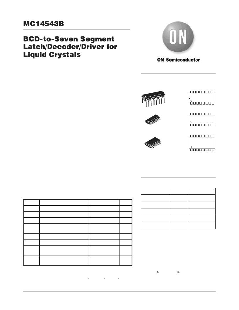
ORDERING INFORMATION
MC14543BCP
PDIP–16
2000/Box
MC14543BD
SOIC–16
48/Rail
MC14543BDR2
SOIC–16
2500/Tape & Reel
1. For ordering information on the EIAJ version of
the SOIC packages, please contact your local
ON Semiconductor representative.
MARKING
DIAGRAMS
16
1
16
PDIP–16
P SUFFIX
CASE 648
MC14543BCP
AWLYYWW
SOIC–16
D SUFFIX
CASE 751B
1
14543B
AWLYWW
SOEIAJ–16
F SUFFIX
CASE 966
1
16
MC14543B
AWLYWW
MC14543BFEL
SOEIAJ–16
See Note 1.
MC14543BF
SOEIAJ–16
See Note 1.
This device contains protection circuitry to guard
against damage due to high static voltages or electric
fields. However, precautions must be taken to avoid ap-
plications of any voltage higher than maximum rated
voltages to this high–impedance circuit. For proper
operation, V
in
and V
out
should be constrained to the
range V
SS
(V
in
or V
out
)
Unused inputs must always be tied to an appropriate
logic voltage level (e.g., either V
SS
or V
DD
). Unused out-
puts must be left open.
V
DD
.
相關PDF資料 |
PDF描述 |
|---|---|
| MC14543BF | Single Channel (1.2V) SVS w/ Watchdog and /MR in 5/SOT23 5-SOT-23 -40 to 85 |
| MC14543BFEL | BCD-to-Seven Segment Latch/Decoder/Driver for Liquid Crystals |
| MC14543B | BCD to Seven Segment Latch/Decoder/Driver for Liquid Crystals(BCD轉七段鎖存/譯碼/驅動(LCD)) |
| MC1455B | Timers |
| MC1455BDG | Timers |
相關代理商/技術參數 |
參數描述 |
|---|---|
| MC14543BDR2G | 功能描述:編碼器、解碼器、復用器和解復用器 3-18V BCD/7-Segment Decoder For LCD’s RoHS:否 制造商:Micrel 產品:Multiplexers 邏輯系列:CMOS 位數: 線路數量(輸入/輸出):2 / 12 傳播延遲時間:350 ps, 400 ps 電源電壓-最大:2.625 V, 3.6 V 電源電壓-最小:2.375 V, 3 V 最大工作溫度:+ 85 C 安裝風格:SMD/SMT 封裝 / 箱體:QFN-44 封裝:Tray |
| MC14543BF | 功能描述:編碼器、解碼器、復用器和解復用器 3-18V BCD/7-Segment RoHS:否 制造商:Micrel 產品:Multiplexers 邏輯系列:CMOS 位數: 線路數量(輸入/輸出):2 / 12 傳播延遲時間:350 ps, 400 ps 電源電壓-最大:2.625 V, 3.6 V 電源電壓-最小:2.375 V, 3 V 最大工作溫度:+ 85 C 安裝風格:SMD/SMT 封裝 / 箱體:QFN-44 封裝:Tray |
| MC14543BFG | 功能描述:編碼器、解碼器、復用器和解復用器 3-18V BCD/7-Segment Decoder For LCD’s RoHS:否 制造商:Micrel 產品:Multiplexers 邏輯系列:CMOS 位數: 線路數量(輸入/輸出):2 / 12 傳播延遲時間:350 ps, 400 ps 電源電壓-最大:2.625 V, 3.6 V 電源電壓-最小:2.375 V, 3 V 最大工作溫度:+ 85 C 安裝風格:SMD/SMT 封裝 / 箱體:QFN-44 封裝:Tray |
| MC145443P | 制造商:Motorola Inc 功能描述: |
| MC145446AFW | 制造商:Rochester Electronics LLC 功能描述:- Bulk 制造商:Motorola Inc 功能描述: 制造商:MOTOROLA 功能描述: |
發布緊急采購,3分鐘左右您將得到回復。