- 您現在的位置:買賣IC網 > PDF目錄382298 > MC145506 (Motorola, Inc.) PCM CODEC FILTER MONO CIRCUIT PDF資料下載
參數資料
| 型號: | MC145506 |
| 廠商: | Motorola, Inc. |
| 元件分類: | Codec |
| 英文描述: | PCM CODEC FILTER MONO CIRCUIT |
| 中文描述: | 單聲道的PCM編解碼器濾波器電路 |
| 文件頁數: | 3/24頁 |
| 文件大小: | 405K |
| 代理商: | MC145506 |
MC145507
MC145508
MOTOROLA
3
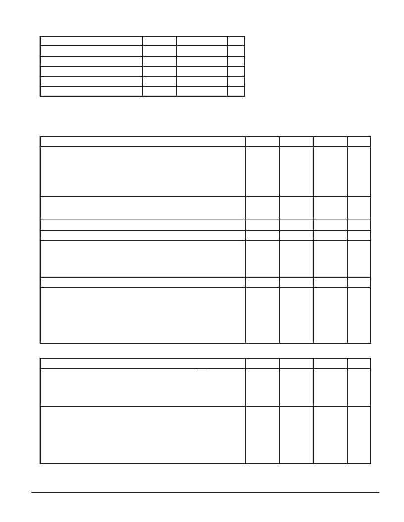
ABSOLUTE MAXIMUM RATINGS
(Voltage Referenced to VSS)
Rating
Symbol
Value
Unit
DC Supply Voltage
VDD – VSS
V
–0.5 to 13
V
Voltage, Any Pin to VSS
DC Drain Per Pin (Excluding VDD, VSS)
Operating Temperature Range
–0.5 to VDD + 0.5
10
V
I
mA
TA
Tstg
–40 to 85
°
C
Storage Temperature Range
–85 to 150
°
C
RECOMMENDED OPERATING CONDITIONS
(TA = –40
°
to 85
°
C)
Characteristic
Min
Typ
Max
Unit
DC Supply Voltage
Dual Supplies: VDD = –VSS (VAG = VLS = 0 V)
Single Supply: VDD to VSS (VAG is an Output, VLS = VDD or VSS)
MC145506, MC145507, MC145508 Using Internal 3.15 V Reference
MC145506 Using Internal 2.5 V Reference
MC145506 Using Internal 3.78 V Reference
MC145506 Using External 1.5 V Reference, Referenced to VAG
4.75
8.5
7.0
9.5
4.75
5.0
—
—
—
—
6.3
12.6
12.6
12.6
12.6
V
Power Dissipation
CMOS Logic Mode (VDD to VSS = 10 V, VLS = VDD)
HCMOS Logic Mode (VDD = 5 V, VSS = –5 V, VLS = VAG = 0 V)
—
—
40
50
70
90
mW
Power Down Dissipation
—
0.1
1.0
mW
Frame Rate Transmit and Receive
7.5
8.0
8.5
kHz
CCI Clock Rate (TDC Clock Rate for MC145507)
MC145506, MC145508
Must Use One of These Frequencies
±
2%, Relative to MSI Frequency of 8 kHz
—
—
—
—
—
128
1536
1544
2048
2560
—
—
—
—
—
kHz
Data Rate for MC145506, MC145508
64
—
4096
kHz
Full Scale Analog Input and Output Level
MC145507, MC145508
MC145506 (Vref = VSS)
RSI = VDD
RSI = VSS
RSI = VAG
RSI = VDD
RSI = VSS
RSI = VAG
MC145506 Using an External Reference Voltage Applied at Vref Pin
—
—
—
—
—
—
—
3.15
3.78
3.15
2.5
1.51 x Vref
1.26 x Vref
Vref
—
—
—
—
—
—
—
VP
DIGITAL LEVELS
(VSS to VDD = 4.75 V to 12.6 V, TA = –40
°
to 85
°
C)
Characteristic
Symbol
Min
Max
Unit
Input Voltage Levels (TDE, TDC, RCE, RDC, RDD, DC, MSI, CCI, PDI)
CMOS Mode (VLS = VDD, VSS is Digital Ground)
“0”
“1”
“0”
“1”
HCMOS Mode (VLS
≤
VDD – 4.0 V, VLS is Digital Ground)
VIL
VIH
VIL
VIH
—
0.7 x VDD
—
VLS + 2.0 V
0.3 x VDD
—
VLS + 0.8 V
—
V
Output Current for TDD (Transmit Digital Data)
CMOS Mode (VLS = VDD, VSS = 0 V and is Digital Ground)
(VDD = 5 V, Vout = 0.4 V)
(VDD = 10 V, Vout = 0.5 V)
(VDD = 5 V, Vout = 4.5 V)
(VDD = 10 V, Vout = 9.5 V)
HCMOS Mode (VLS
≤
VDD – 4.75 V, VLS = 0 V and is Digital Ground) (VOL = 0.4 V)
(VOH = VDD – 0.5 V)
IOL
IOH
IOL
IOH
1.6
1.6
–1.6
–1.6
1.6
–1.6
—
—
—
—
—
—
mA
This device contains circuitry to protect
against damage due to high static voltages or
electric fields; however, it is advised that
normal precautions be taken to avoid applica-
tion of any voltage higher than maximum rated
voltages to this high–impedance circuit. For
proper operation, it is recommended that Vin
and Vout be constrained to the range VSS
≤
(Vin or Vout)
≤
VDD.
Unused inputs must always be tied to an
appropriate logic voltage level (e.g., VSS,
VDD, VLS, or VAG).
F
Freescale Semiconductor, Inc.
For More Information On This Product,
Go to: www.freescale.com
n
.
相關PDF資料 |
PDF描述 |
|---|---|
| MC145507 | PCM CODEC FILTER MONO CIRCUIT |
| MC145508 | PCM CODEC FILTER MONO CIRCUIT |
| MC14551BCP | Quad 2-Channel Analog Multiplexer/Demultiplexer |
| MC14551BD | Quad 2-Channel Analog Multiplexer/Demultiplexer |
| MC14551BDR2 | Quad 2-Channel Analog Multiplexer/Demultiplexer |
相關代理商/技術參數 |
參數描述 |
|---|---|
| MC145506P | 制造商:Rochester Electronics LLC 功能描述:LOW VOLTAGE COMPANDER - Bulk |
| MC14551 C38E WAF | 制造商:ON Semiconductor 功能描述: |
| MC14551BCP | 功能描述:多路器開關 IC 3-18V Quad 2 CHNL RoHS:否 制造商:Texas Instruments 通道數量:1 開關數量:4 開啟電阻(最大值):7 Ohms 開啟時間(最大值): 關閉時間(最大值): 傳播延遲時間:0.25 ns 工作電源電壓:2.3 V to 3.6 V 工作電源電流: 最大工作溫度:+ 85 C 安裝風格:SMD/SMT 封裝 / 箱體:UQFN-16 |
| MC14551BCPG | 功能描述:多路器開關 IC 3-18V Quad 2 CHNL Mux/Demux -55 to 125 RoHS:否 制造商:Texas Instruments 通道數量:1 開關數量:4 開啟電阻(最大值):7 Ohms 開啟時間(最大值): 關閉時間(最大值): 傳播延遲時間:0.25 ns 工作電源電壓:2.3 V to 3.6 V 工作電源電流: 最大工作溫度:+ 85 C 安裝風格:SMD/SMT 封裝 / 箱體:UQFN-16 |
| MC14551BD | 功能描述:多路器開關 IC 3-18V Quad 2 CHNL RoHS:否 制造商:Texas Instruments 通道數量:1 開關數量:4 開啟電阻(最大值):7 Ohms 開啟時間(最大值): 關閉時間(最大值): 傳播延遲時間:0.25 ns 工作電源電壓:2.3 V to 3.6 V 工作電源電流: 最大工作溫度:+ 85 C 安裝風格:SMD/SMT 封裝 / 箱體:UQFN-16 |
發布緊急采購,3分鐘左右您將得到回復。