- 您現在的位置:買賣IC網 > PDF目錄371031 > MC33066DW (MOTOROLA INC) HIGH PERFORMANCE RESONANT MODE CONTROLLERS PDF資料下載
參數資料
| 型號: | MC33066DW |
| 廠商: | MOTOROLA INC |
| 元件分類: | 穩壓器 |
| 英文描述: | HIGH PERFORMANCE RESONANT MODE CONTROLLERS |
| 中文描述: | 1.5 A SWITCHING CONTROLLER, 1000 kHz SWITCHING FREQ-MAX, PDSO16 |
| 封裝: | PLASTIC, SO-16 |
| 文件頁數: | 3/12頁 |
| 文件大小: | 168K |
| 代理商: | MC33066DW |
MC34066 MC33066
3
MOTOROLA ANALOG IC DEVICE DATA
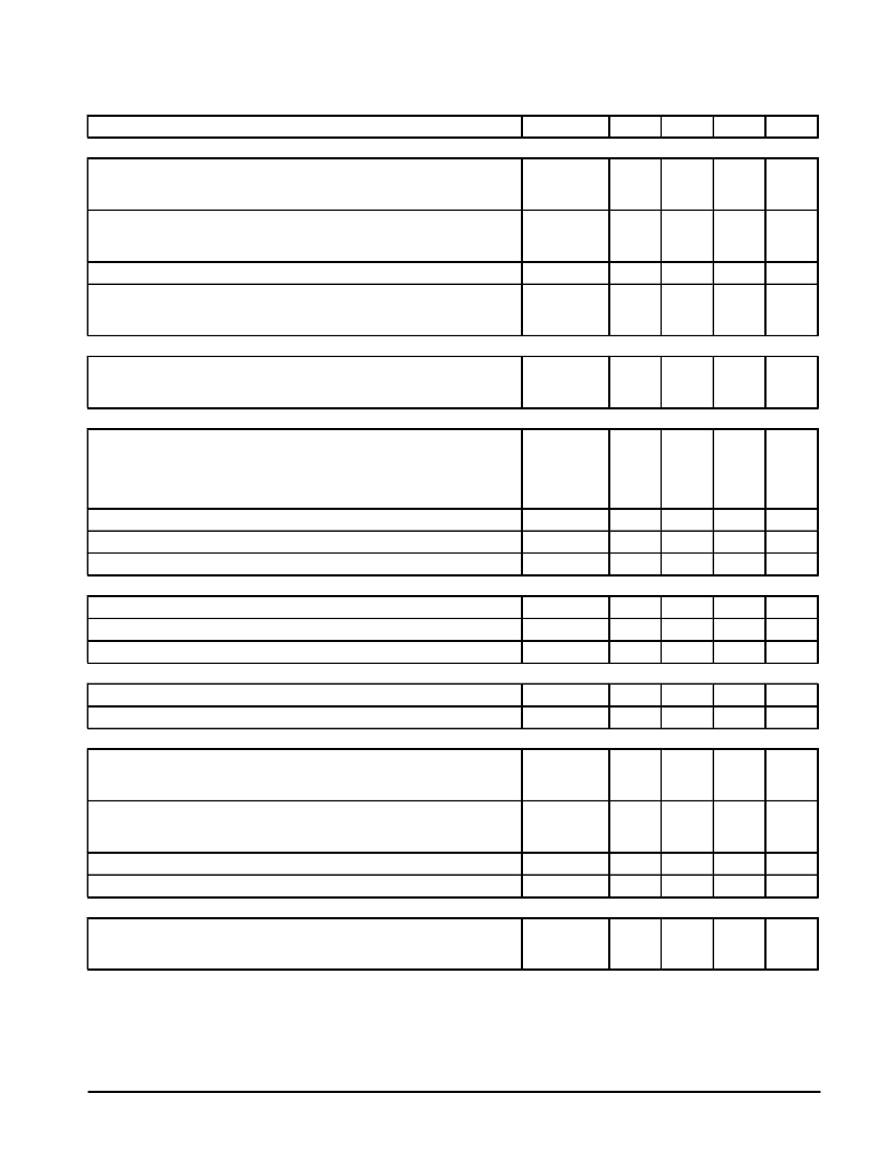
ELECTRICAL CHARACTERISTICS (continued)
(VCC = 12 V [Note 2], ROSC = 95.3 k, RDT = 0
, RVFO = 5.62 k, COSC = 300 pF,
RT = 14.3 k, CT = 300 pF, CL = 1.0 nF, for typical values TA = 25
°
C, for min/max values TA is the operating ambient temperature range that
applies [Note 3], unless otherwise noted.)
Characteristics
Symbol
Min
Typ
Max
Unit
OSCILLATOR
Frequency (Error Amp Output Low)
TA = 25
°
C
Total Variation (VCC = 10 V to 18 V, TA = TLow to THigh)
fOSC(low)
90
85
100
–
110
115
kHz
Frequency (Error Amp Output High)
TA = 25
°
C
Total Variation (VCC = 10 V to 18 V, TA = TLow to THigh)
Oscillator Control Input Voltage, Pin 3 (ISink = 0.5 mA, TA = 25
°
C)
Output Deadtime (Error Amp Output High)
RDT = 0
RDT = 1.0 k
fOSC(high)
900
850
1000
–
1100
1150
kHz
Vin
DT
1.3
1.4
1.5
V
–
600
70
700
100
800
ns
ONE–SHOT
Drive Output On–Time (RDT = 1.0 k)
TA = 25
°
C
Total Variation (VCC = 10 V to 18 V, TA = TLow to THigh)
tOS
1.43
1.4
1.5
–
1.57
1.6
μ
s
DRIVE OUTPUTS
Output Voltage
Low State (ISink = 20 mA)
Low State
(ISink = 200 mA)
High State (ISource = 20 mA)
High State
(ISource = 200 mA)
Output Voltage with UVLO Activated (VCC = 6.0 V, ISink = 1.0 mA)
Output Voltage Rise Time (CL = 1.0 nF)
Output Voltage Fall Time (CL = 1.0 nF)
VOL
VOH
–
–
9.5
9.0
0.8
1.5
10.3
9.8
1.2
2.0
–
–
V
VOL(UVLO)
tr
tf
–
0.8
1.2
V
–
20
50
ns
–
20
50
ns
FAULT COMPARATOR
Input Threshold
Vth
IIB
0.95
1.0
1.05
V
Input Bias Current (VPin 10 = 0 V)
Propagation Delay to Drive Outputs (100 mV Overdrive)
–
–2.0
–10
μ
A
tPLH(In/Out)
–
60
100
ns
SOFT–START
Capacitor Charge Current (VPin 11 = 2.5 V)
Capacitor Discharge Current (VPin 11 = 2.5 V)
Ichg
IIdchg
4.5
8.1
14
μ
A
1.0
8.0
–
mA
UNDERVOLTAGE LOCKOUT
Startup Threshold, VCC Increasing
Enable/UVLO Adjust Pin Open
Enable/UVLO Adjust Pin Connected to VCC
Vth(UVLO)
14.8
8.0
16
9.0
17.2
10
V
Minimum Operating Voltage after Turn–On
Enable/UVLO Adjust Pin Open
Enable/UVLO Adjust Pin Connected to VCC
VCC(min)
8.0
7.6
9.0
8.6
10
9.6
V
Enable/UVLO Adjust Shutdown Threshold Voltage
Vth(Enable)
Iin(Enable)
6.0
7.0
–
V
Enable/UVLO Adjust Input Current (Pin 9 = 0V)
–
–0.2
–1.0
mA
TOTAL DEVICE
Power Supply Current (Enable/UVLO Adjust Pin Open)
Startup (VCC = 13.5 V)
Operating (fOSC = 100 kHz) (Note 2)
ICC
–
–
0.45
21
0.6
30
mA
NOTES:
2.Adjust VCC above the Startup threshold before setting to 12 V.
3.Low duty cycle pulse techniques are used during test to maintain junction temperature as close to ambient as possible.
Tlow= 0
°
C for MC34066
Thigh=
–40
°
C for MC33066
Thigh=
+70
°
C for MC34066
+85
°
C for MC33066
相關PDF資料 |
PDF描述 |
|---|---|
| MC33066P | HIGH PERFORMANCE RESONANT MODE CONTROLLERS |
| MC34066P | Enhanced Product Single Voltage Detectors 5-SC70 -55 to 125 |
| MC33066 | HIGH PERFORMANCE RESONANT MODE CONTROLLERS |
| MC34066 | HIGH PERFORMANCE RESONANT MODE CONTROLLERS |
| MC34080 | Low Quiescent Current, Programmable-Delay Supervisory Circuit 6-SOT-23 -40 to 125 |
相關代理商/技術參數 |
參數描述 |
|---|---|
| MC33066P | 制造商:MOTOROLA 制造商全稱:Motorola, Inc 功能描述:High Performance Resonant Mode Controllers |
| MC33067 | 制造商:ONSEMI 制造商全稱:ON Semiconductor 功能描述:High Performance Resonant Mode Controllers |
| MC33067-34067CN | 制造商:未知廠家 制造商全稱:未知廠家 功能描述:中文資料 |
| MC33067DW | 功能描述:DC/DC 開關控制器 High Performance RoHS:否 制造商:Texas Instruments 輸入電壓:6 V to 100 V 開關頻率: 輸出電壓:1.215 V to 80 V 輸出電流:3.5 A 輸出端數量:1 最大工作溫度:+ 125 C 安裝風格: 封裝 / 箱體:CPAK |
| MC33067DWG | 功能描述:DC/DC 開關控制器 High Performance Resonant Mode RoHS:否 制造商:Texas Instruments 輸入電壓:6 V to 100 V 開關頻率: 輸出電壓:1.215 V to 80 V 輸出電流:3.5 A 輸出端數量:1 最大工作溫度:+ 125 C 安裝風格: 封裝 / 箱體:CPAK |
發布緊急采購,3分鐘左右您將得到回復。