- 您現在的位置:買賣IC網 > PDF目錄371031 > MC33066P (MOTOROLA INC) HIGH PERFORMANCE RESONANT MODE CONTROLLERS PDF資料下載
參數資料
| 型號: | MC33066P |
| 廠商: | MOTOROLA INC |
| 元件分類: | 穩壓器 |
| 英文描述: | HIGH PERFORMANCE RESONANT MODE CONTROLLERS |
| 中文描述: | 1.5 A SWITCHING CONTROLLER, 1000 kHz SWITCHING FREQ-MAX, PDIP16 |
| 封裝: | PLASTIC, DIP-16 |
| 文件頁數: | 4/12頁 |
| 文件大小: | 168K |
| 代理商: | MC33066P |
MC34066 MC33066
4
MOTOROLA ANALOG IC DEVICE DATA
VCC
15
9
Enable/
UVLO Adjust
Osc Deadtime
1
RDT
ROSC
COSC
Osc RC
2
One–Shot RC
16
CT
RT Osc Control
Current
3
IOSC
RVFO
Error Amp
Output
Error Amp
Inverting Input
Error Amp
Noninverting Input
6
7
8
CSoft–Start
11
7k
50k
7k
50k
Reference
Regulator
5.1V
Vref UVLO
8VVCC UVLO
UVLO
VCC
4.2V/4V
Q1
Q2
Drivers
5.1V
Oscillator
Steering
Flip–Flop
IOSC
4.9V/3.6V
ton
T
Q
Q
R
One–Shot
–
+
4.9V/3.6V
UVLO + Fault
Fault
Comparator
Q
R
S
Current Mirror
Error Amp
Output Clamp
Fault
Fault
Latch
1.0V
2.5V
EA Clamp
Soft–Start
Buffer
9
μ
A
Error
Amplifier
Vref
Gnd
5
4
14
12
13
10
Drive
Output B
Drive
Gnd
Fault
Input
–
+
+
–
+
–
–
+
+
–
+
–
Drive
Output A
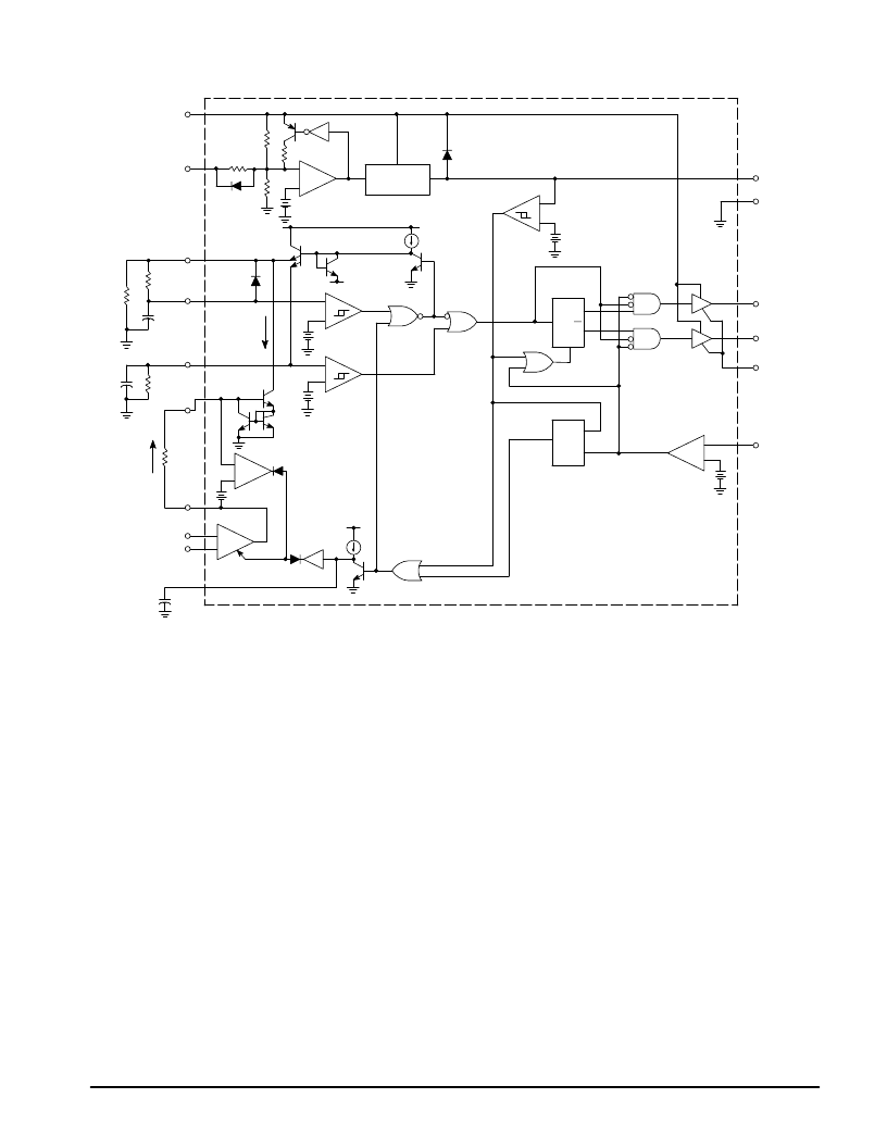
Figure 1. MC34066 Representative Block Diagram
OPERATING DESCRIPTION
Introduction
As power supply designers have strived to increase power
conversion efficiency and reduce passive component size,
high frequency resonant mode power converters have
emerged as attractive alternatives to conventional
square–wave control. When compared to square–wave
converters, resonant mode control offers several benefits
including lower switching losses, higher efficiency, lower EMI
emission, and smaller size. This integrated circuit has been
developed to support new trends in power supply design.
The MC34066 Resonant Mode Controller is a high
performance bipolar IC dedicated to variable frequency
power control at frequencies exceeding 1.0 MHz. This
integrated circuit provides the features, performance and
flexibility for a wide variety of resonant mode power supply
applications.
The primary purpose of the control chip is to supply
precise pulses to the gates of external power MOSFETs at a
repetition rate regulated by a feedback control loop. The
MC34066 can be operated in any of three modes as follows:
1) fixed on–time, variable frequency; 2) fixed off–time,
variable frequency; and 3) combinations of 1 and 2 that
change from fixed on–time to fixed off–time as the frequency
increases. Additional features of the IC ensure that system
startup and fault conditions are administered in a safe,
controlled manner.
A simplified block diagram of the IC is shown on the first
page of this data sheet, which identifies the main functional
blocks and the block–to–block interconnects. Figure 1 is a
detailed functional diagram which accurately represents the
internal circuitry. The various functions can be divided into
two sections. The first section includes the primary control
path which produces precise output pulses at the desired
frequency Oscillator, a One–Shot, a pulse Steering Flip–Flop,
a pair of power MOSFET Drivers, and a wide bandwidth Error
Amplifier. The second section provides several peripheral
support functions including a voltage reference, undervoltage
lockout, Soft–Start circuit, and a fault detector.
Primary Control Path
The output pulse width and repetition rate are regulated
through the interaction of the variable frequency Oscillator,
One–Shot timer and Error Amplifier. The Oscillator triggers
the One–Shot which generates a pulse that is alternately
steered to a pair of totem–pole output drivers by a toggle
Flip–Flop. The Error Amplifier monitors the output of the
regulator and modulates the frequency of the Oscillator.
High–speed Schottky logic is used throughout the primary
control channel to minimize delays and enhance high
frequency characteristics.
相關PDF資料 |
PDF描述 |
|---|---|
| MC34066P | Enhanced Product Single Voltage Detectors 5-SC70 -55 to 125 |
| MC33066 | HIGH PERFORMANCE RESONANT MODE CONTROLLERS |
| MC34066 | HIGH PERFORMANCE RESONANT MODE CONTROLLERS |
| MC34080 | Low Quiescent Current, Programmable-Delay Supervisory Circuit 6-SOT-23 -40 to 125 |
| MC34081BD | Low Quiescent Current, Programmable-Delay Supervisory Circuit 6-SOT-23 -40 to 125 |
相關代理商/技術參數 |
參數描述 |
|---|---|
| MC33067 | 制造商:ONSEMI 制造商全稱:ON Semiconductor 功能描述:High Performance Resonant Mode Controllers |
| MC33067-34067CN | 制造商:未知廠家 制造商全稱:未知廠家 功能描述:中文資料 |
| MC33067DW | 功能描述:DC/DC 開關控制器 High Performance RoHS:否 制造商:Texas Instruments 輸入電壓:6 V to 100 V 開關頻率: 輸出電壓:1.215 V to 80 V 輸出電流:3.5 A 輸出端數量:1 最大工作溫度:+ 125 C 安裝風格: 封裝 / 箱體:CPAK |
| MC33067DWG | 功能描述:DC/DC 開關控制器 High Performance Resonant Mode RoHS:否 制造商:Texas Instruments 輸入電壓:6 V to 100 V 開關頻率: 輸出電壓:1.215 V to 80 V 輸出電流:3.5 A 輸出端數量:1 最大工作溫度:+ 125 C 安裝風格: 封裝 / 箱體:CPAK |
| MC33067DWR2 | 功能描述:DC/DC 開關控制器 High Performance RoHS:否 制造商:Texas Instruments 輸入電壓:6 V to 100 V 開關頻率: 輸出電壓:1.215 V to 80 V 輸出電流:3.5 A 輸出端數量:1 最大工作溫度:+ 125 C 安裝風格: 封裝 / 箱體:CPAK |
發布緊急采購,3分鐘左右您將得到回復。