- 您現在的位置:買賣IC網 > PDF目錄382301 > MC33121P (MOTOROLA INC) LOW VOLTAGE SUBSCRIBER LOOP INTERFACE CIRCUIT PDF資料下載
參數資料
| 型號: | MC33121P |
| 廠商: | MOTOROLA INC |
| 元件分類: | 模擬傳輸電路 |
| 英文描述: | LOW VOLTAGE SUBSCRIBER LOOP INTERFACE CIRCUIT |
| 中文描述: | TELECOM-SLIC, PDIP20 |
| 封裝: | PLASTIC, DIP-20 |
| 文件頁數: | 19/32頁 |
| 文件大小: | 570K |
| 代理商: | MC33121P |
第1頁第2頁第3頁第4頁第5頁第6頁第7頁第8頁第9頁第10頁第11頁第12頁第13頁第14頁第15頁第16頁第17頁第18頁當前第19頁第20頁第21頁第22頁第23頁第24頁第25頁第26頁第27頁第28頁第29頁第30頁第31頁第32頁
MC33121
MOTOROLA
19
The receive gain (GRX), defined as the voltage gain from
VRX to VL, is calculated as follows:
RXI is a virtual ground, and Rac is the AC impedance of
the load (phone line).
The AC current generated in the transistors is 102
IRXI,
which is equal to 102
(IR – ITXO).
IR = VRX/RRX, and
VTXO
RRO
RRO
(31 k
ITXO
VL
31 k
0.328
RC)
(10)
Using equations 5 and 8, involving Zac, RS and RC, and
the above equations yields:
VL
VRX
GRX
102
(Rac
Zac)
RRX
(11)
Therefore, RRX
102
(Rac
Zac)
GRX
(12)
Equation 12 applies
only
for the case where Rac and Zac
have the same configuration. If they also have the same
magnitude, then set RRX = 51
Rac to set a receive gain of
0 dB. The AC source impedance of the above circuit to Tip
and Ring is Zac. For the case where Rac
≠
Zac, use the fol-
lowing equation:
VL
VRX
102
RRX
1
ZL
1.037
106
(31 k
RC)
RRO
(13)
where ZL
Rac
2
RS
(RC
31 k)
2
(14)
a) Resistive Loads
For a 600
resistive system, set RRX = 30.6 k
, and for
a 900
resistive system, set RRX = 45.9 k
.
b) Complex Loads
For complex (nonresistive) loads, the RRX resistor needs
to be replaced with a network having the same configuration
as the complex load, but with all impedance values scaled up
by a factor of 51 (for 0 dB gain). If a gain other than 0 dB is
desired, the scaling factor is determined from Equation 12.
This method applies
only
if the RRO network has been
made complex comparable to the load according to the pro-
cedure in the previous section (Equations 5 – 9a), such that
Rac = Zac. Using a scaling factor of 51, and the previous ex-
amples, yields:
IF THE AC LOAD IS:
THEN RRX SHOULD BE:
900
TO TIP
AND RING
TO
RXI
820
IF THE AC LOAD IS:
THEN RRX SHOULD BE:
TO TIP
AND RING
TO
RXI
220
VRX
45.9 k
42 nF
2.25 nF
11.2 k
41.8 k
VRX
0.115
μ
F
2.16
μ
F
The preceding procedure will yield a receive gain which is
constant with respect to frequency. The RRX resistor, or net-
work, must have a tolerance equal to or better than the re-
quired system tolerance for receive gain.
7) Transmit Gain (GTX)
Setting the transmit gain involves selecting RTX1 and RTX2
in Figure 28. The voltage gain from VL to VTX is calculated
from the following:
GTX
VTX
VL
RTX2
31 k
0.328
RTX1
(RC
31 k)
(15)
For 0 dB gain, set RTX2 = 3.15 x RTX1 (for RC = 1.0 k). The
actual values of RTX2 and RTX1 are not critical — only their
ratio so as to provide the proper gain at the op amp. Once the
ratio is established, the two resistors can be selected from a
set of standard resistor values. The minimum value for RTX1
is limited by the drive capability of TXO, which is a nominal
±
800
μ
A peak (
±
275
μ
A minimum). As a general rule, RTX1
should be between 5.0 k
and 20 k
. The load on TXO is
the parallel combination of RTX1 and RRO.
CTX is for DC blocking, and is typically a large value
(1.0
μ
F) so as to not be a significant impedance. In general,
it should
not
be used for low frequency rolloff as that will af-
fect the transhybrid rejection (discussed in the next section).
Low frequency rolloff should be done after the op amp. High
frequency roll–off can be set by placing a capacitor across
RTX2.
For complex loads (at Tip and Ring), if RRO and RRX have
been made complex comparable to the load as described in
the previous sections, neither RTX1 nor RTX2 needs to be
complex since both the transmit and receive signals which
appear at TXO will be flat with respect to frequency.
RTX1 and RTX2 must have a tolerance equal to or better
than the required system tolerance for the transmit gain.
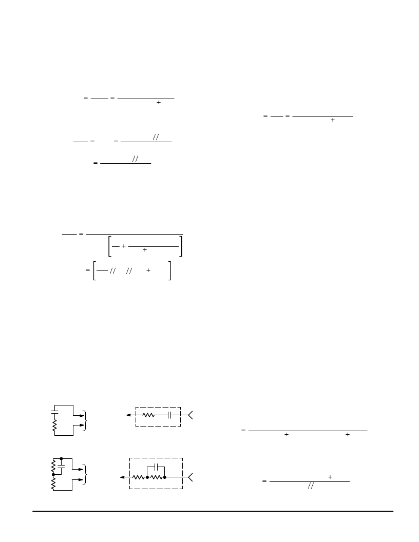
8) Balance Network (RB) — Transhybrid Rejection
When a receive signal is applied to VRX to produce a sig-
nal at Tip and Ring, the two–to–four wire arrangement of a
hybrid (the MC33121) results in a reflected signal at TXO.
Transhybrid rejection involves canceling that reflected signal
before it appears at VTX. The method used is to insert the RB
resistor (or network) as shown in Figure 36. The current IB,
supplied from VRX, cancels the current ITX1 supplied from
TXO (Node A is a virtual ground). Good transhybrid cancella-
tion requires that the currents be equal in magnitude
and
180
°
out of phase at Node A.
Using the equations for transmit and receive gains, the
current ITX1 is equal to:
ITX1
33.5
VRX
Zac
ZL
31 k
RRX
[Zac
ZL]
RTX1
(RC
31 k)
(16)
a) For the case where RRO and RRX are comparable in
configuration to Z:
Since IB = VRX/RB, then RB can be determined from:
RRX
RTX1
(RC
33.5
[Zac
RB
31 k)
ZL]
31 k
(17)
相關PDF資料 |
PDF描述 |
|---|---|
| MC33151 | High Speed Dual MOSFET Drivers |
| MC33151DR2 | High Speed Dual MOSFET Drivers |
| MC34151DR2 | High Speed Dual MOSFET Drivers |
| MC33151VDR2 | 0.022 UF 10% 50V X7R (0603) CAP TR |
| MC33151D | High Speed Dual MOSFET Drivers |
相關代理商/技術參數 |
參數描述 |
|---|---|
| MC33128 | 制造商:MOTOROLA 制造商全稱:Motorola, Inc 功能描述:POWER MANAGEMENT CONTROLLER |
| MC33128D | 制造商:MOTOROLA 制造商全稱:Motorola, Inc 功能描述:POWER MANAGEMENT CONTROLLER |
| MC33129 | 制造商:FREESCALE 制造商全稱:Freescale Semiconductor, Inc 功能描述:High Performance Current Mode Controllers |
| MC33129D | 制造商:Motorola Inc 功能描述: |
| MC33129DR2 | 制造商: 功能描述: 制造商:undefined 功能描述: |
發布緊急采購,3分鐘左右您將得到回復。