- 您現在的位置:買賣IC網 > PDF目錄382301 > MC33151 (ON SEMICONDUCTOR) High Speed Dual MOSFET Drivers PDF資料下載
參數資料
| 型號: | MC33151 |
| 廠商: | ON SEMICONDUCTOR |
| 英文描述: | High Speed Dual MOSFET Drivers |
| 中文描述: | 高速雙MOSFET驅動器 |
| 文件頁數: | 6/12頁 |
| 文件大?。?/td> | 284K |
| 代理商: | MC33151 |
MC34151, MC33151
http://onsemi.com
6
the NPN pull–up during the negative output transient, power
dissipation at high frequencies can become excessive.
Figures 19, 20, and 21 show a method of using external
Schottky diode clamps to reduce driver power dissipation.
Undervoltage Lockout
An undervoltage lockout with hysteresis prevents erratic
system operation at low supply voltages. The UVLO forces
the Drive Outputs into a low state as VCC rises from 1.4 V
to the 5.8 V upper threshold. The lower UVLO threshold is
5.3 V, yielding about 500 mV of hysteresis.
Power Dissipation
Circuit performance and long term reliability are
enhanced with reduced die temperature. Die temperature
increase is directly related to the power that the integrated
circuit must dissipate and the total thermal resistance from
the junction to ambient. The formula for calculating the
junction temperature with the package in free air is:
TJ = TA + PD (R
θ
JA)
where:
TJ = Junction Temperature
TA = Ambient Temperature
PD = Power Dissipation
R
θ
JA =Thermal Resistance Junction to Ambient
There are three basic components that make up total
power to be dissipated when driving a capacitive load with
respect to ground. They are:
PD =PQ + PC + PT
where:
PQ = Quiescent Power Dissipation
PC = Capacitive Load Power Dissipation
PT = Transition Power Dissipation
The quiescent power supply current depends on the
supply voltage and duty cycle as shown in Figure 16. The
device’s quiescent power dissipation is:
PQ = VCC
ICCL (1–D) + ICCH (D)
where:
ICCL = Supply Current with Low State Drive
Outputs
ICCH = Supply Current with High State Drive
Outputs
D = Output Duty Cycle
The capacitive load power dissipation is directly related
to the load capacitance value, frequency, and Drive Output
voltage swing. The capacitive load power dissipation per
driver is:
PC = VCC (VOH – VOL) CL f
where:
VOH = High State Drive Output Voltage
VOL = Low State Drive Output Voltage
CL = Load Capacitance
f = frequency
When driving a MOSFET, the calculation of capacitive
load power PC is somewhat complicated by the changing
gate to source capacitance CGS as the device switches. To aid
in this calculation, power MOSFET manufacturers provide
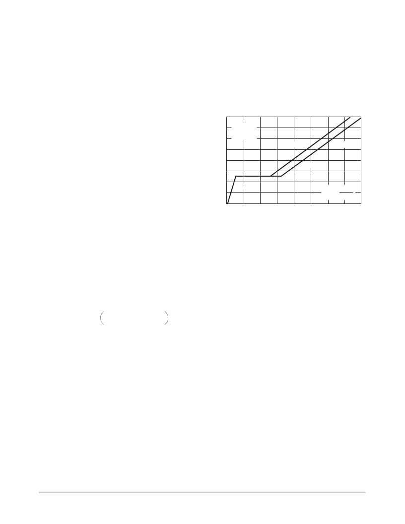
gate charge information on their data sheets. Figure 17
shows a curve of gate voltage versus gate charge for the ON
Semiconductor MTM15N50. Note that there are three
distinct slopes to the curve representing different input
capacitance values. To completely switch the MOSFET
‘on’, the gate must be brought to 10 V with respect to the
source. The graph shows that a gate charge Qg of 110 nC is
required when operating the MOSFET with a drain to source
voltage VDS of 400 V.
V
Qg, GATE CHARGE (nC)
CGS =
Qg
VGS
16
12
8.0
4.0
00
40
80
120
160
VDS = 100 V
VDS = 400 V
8.9 nF
2.0 nF
MTM15N50
ID = 15 A
TA = 25
°
C
Figure 17. Gate–To–Source Voltage
versus Gate Charge
The capacitive load power dissipation is directly related to
the required gate charge, and operating frequency. The
capacitive load power dissipation per driver is:
PC(MOSFET) = VC Qg f
The flat region from 10 nC to 55 nC is caused by the
drain–to–gate Miller capacitance, occurring while the
MOSFET is in the linear region dissipating substantial
amounts of power. The high output current capability of the
MC34151 is able to quickly deliver the required gate charge
for fast power efficient MOSFET switching. By operating
the MC34151 at a higher VCC, additional charge can be
provided to bring the gate above 10 V. This will reduce the
‘on’ resistance of the MOSFET at the expense of higher
driver dissipation at a given operating frequency.
The transition power dissipation is due to extremely short
simultaneous conduction of internal circuit nodes when the
Drive Outputs change state. The transition power
dissipation per driver is approximately:
PT 9 VCC (1.08 VCC CL f – 8 y 10–4)
PT must be greater than zero.
Switching time characterization of the MC34151 is
performed with fixed capacitive loads. Figure 13 shows that
for small capacitance loads, the switching speed is limited
by transistor turn–on/off time and the slew rate of the
internal nodes. For large capacitance loads, the switching
speed is limited by the maximum output current capability
of the integrated circuit.
相關PDF資料 |
PDF描述 |
|---|---|
| MC33151DR2 | High Speed Dual MOSFET Drivers |
| MC34151DR2 | High Speed Dual MOSFET Drivers |
| MC33151VDR2 | 0.022 UF 10% 50V X7R (0603) CAP TR |
| MC33151D | High Speed Dual MOSFET Drivers |
| MC33151P | High Speed Dual MOSFET Drivers |
相關代理商/技術參數 |
參數描述 |
|---|---|
| MC33151 | 制造商:SPC Multicomp 功能描述:PTC Resettable Fuse |
| MC33151D | 功能描述:功率驅動器IC 1.5A High Speed Dual RoHS:否 制造商:Micrel 產品:MOSFET Gate Drivers 類型:Low Cost High or Low Side MOSFET Driver 上升時間: 下降時間: 電源電壓-最大:30 V 電源電壓-最小:2.75 V 電源電流: 最大功率耗散: 最大工作溫度:+ 85 C 安裝風格:SMD/SMT 封裝 / 箱體:SOIC-8 封裝:Tube |
| MC33151DG | 功能描述:功率驅動器IC 1.5A High Speed Dual Inverting MOSFET RoHS:否 制造商:Micrel 產品:MOSFET Gate Drivers 類型:Low Cost High or Low Side MOSFET Driver 上升時間: 下降時間: 電源電壓-最大:30 V 電源電壓-最小:2.75 V 電源電流: 最大功率耗散: 最大工作溫度:+ 85 C 安裝風格:SMD/SMT 封裝 / 箱體:SOIC-8 封裝:Tube |
| MC33151DR2 | 功能描述:功率驅動器IC 1.5A High Speed Dual RoHS:否 制造商:Micrel 產品:MOSFET Gate Drivers 類型:Low Cost High or Low Side MOSFET Driver 上升時間: 下降時間: 電源電壓-最大:30 V 電源電壓-最小:2.75 V 電源電流: 最大功率耗散: 最大工作溫度:+ 85 C 安裝風格:SMD/SMT 封裝 / 箱體:SOIC-8 封裝:Tube |
| MC33151DR2G | 功能描述:功率驅動器IC 1.5A High Speed Dual Inverting MOSFET RoHS:否 制造商:Micrel 產品:MOSFET Gate Drivers 類型:Low Cost High or Low Side MOSFET Driver 上升時間: 下降時間: 電源電壓-最大:30 V 電源電壓-最小:2.75 V 電源電流: 最大功率耗散: 最大工作溫度:+ 85 C 安裝風格:SMD/SMT 封裝 / 箱體:SOIC-8 封裝:Tube |
發布緊急采購,3分鐘左右您將得到回復。