- 您現在的位置:買賣IC網 > PDF目錄371029 > MC33389DDW (MOTOROLA INC) System Basis Chip with Low Speed Fault Tolerant CAN PDF資料下載
參數資料
| 型號: | MC33389DDW |
| 廠商: | MOTOROLA INC |
| 元件分類: | 網絡接口 |
| 英文描述: | System Basis Chip with Low Speed Fault Tolerant CAN |
| 中文描述: | DATACOM, INTERFACE CIRCUIT, PDSO28 |
| 封裝: | PLASTIC, SO-28 |
| 文件頁數: | 1/35頁 |
| 文件大小: | 609K |
| 代理商: | MC33389DDW |
當前第1頁第2頁第3頁第4頁第5頁第6頁第7頁第8頁第9頁第10頁第11頁第12頁第13頁第14頁第15頁第16頁第17頁第18頁第19頁第20頁第21頁第22頁第23頁第24頁第25頁第26頁第27頁第28頁第29頁第30頁第31頁第32頁第33頁第34頁第35頁
7
28
2
Advance Information
System Basis Chip with Low
Speed Fault Tolerant CAN
This document contains information on a new product under development. Motorola reserves the
right to change or discontinue this product without notice.
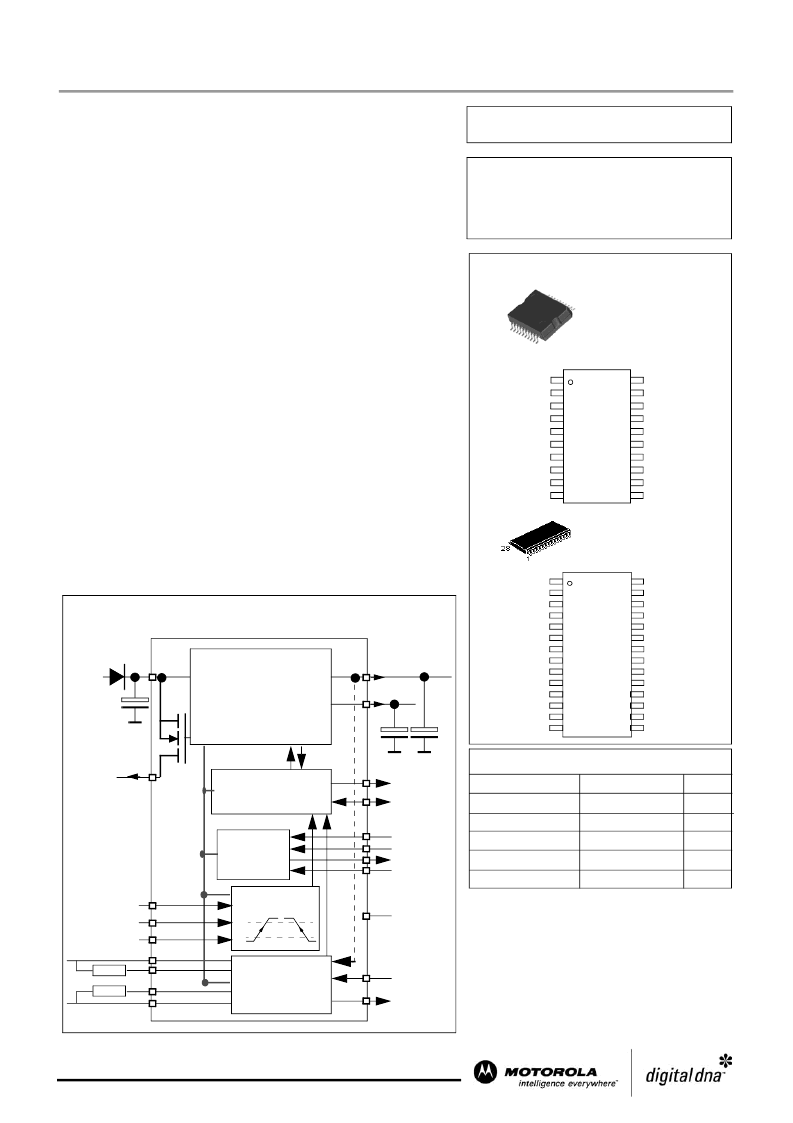
Simplified Block Diagram
Interrupt control
Reset control
Watchdog & oscillator
Programmable
wake-up inputs
SPI Interface
Dual Voltage Regulator
Voltage control
Bat fail detect
VCC monitor
VBAT switch supply
Mode control
Gnd
RX
TX
Fault tolerant
CAN
transceiver
CSB
MISO
SCK
MOSI
Reset
INT
5V
V2
V1
max 200mA
max 110mA
I3 max. 100mA
Wake-up
inputs
L0
L1
L2
R1
R2
VBAT
(+12V)
V3
(Switch supply)
CAN L
5V
Rth
Rtl
CAN H
MC33389
Semiconductor Technical Data
MOTOROLA
Order Number: MC33389/D
Rev 3.5, March 17th, 03
Motorola, Inc., 2002. All rights reserved.
1
2
3
5
4
6
7
8
9
10
1
2
3
3
4
4
5
6
1
1
1
1
2
2
2
2
DH SUFFIX
POWER PACKAGE
CASE 979C
HSOP-20
V1
RX
MOSI
SCK
CSB
MISO
RSTB
INTB
GND
GND
GND
GND
V2
CANH
GND
V3
VBAT
RTL
CANL
RTH
NC
GND
L2
L1
TX
L0
GND
GND
5
6
7
8
9
20
1
1
1
1
1
2
2
1
2
AUTOMOTIVE SBC
SYSTEM BASIS CHIP
SILICON MONOLITHIC
INTEGRATED CIRCUIT
V1
RX
MOSI
SCK
CSB
L2
MISO
RSTB
INTB
TX
V2
CANH
GND
V3
VBAT
RTL
CANL
RTH
L0
L1
1
2
3
5
4
6
7
8
9
10
1
2
3
5
4
6
7
8
9
20
1
1
1
1
1
1
1
1
1
ORDERING INFORMATION
Device and version
Operating
Temperature Range
Package
SO-28
T
A
= -40 to 125°C
MC33389ADW (1)
PIN CONNECTIONS
MC33389ADH (1) T
A
= -40 to 125°C
DW SUFFIX
PLASTIC PACKAGE
CASE 751F
SO-28
(1) Version A: If device remains in reset greater than 100ms due
to V1 undervoltage, device switches to sleep mode to minimise
current consumption. Wake-up configuration active.
(2) Version C: In V1 undervoltage condition, device remains in
permanent reset state until V1 returns to nominal conditions. V1
protected by overcurrent and over temperature functions.
(3) Version D: In V1 undervoltage condition, device remains in
permanent reset state until V1 returns to nominal conditions. V1
protected by overcurrent and over temperature functions.
Change of undervoltage reset threshold. Refer to electrical pa-
rameter table, V1 PIn 5V.
MC33389CDW (2) T
A
= -40 to 125°C
MC33389CDH (2) T
A
= -40 to 125°C
HSOP20
HSOP20
SO-28
MC33389DDW (3) T
A
= -40 to 125°C
SO-28
The MC33389 is a monolithic integrated circuit combining many functions
frequently used by automotive ECUs. It incorporates a low speed fault tolerant
CAN transceiver.
Dual Low Drop Voltage Regulators, with Respectively 100mA and 200mA
Current Capabilities, Current Limitation and Over Temperature Detection with
Prewarning
5V Output Voltage for V1 Regulator
Three Operational Modes (Normal, Standby and Sleep Mode) Separated
from the CAN Interface Operating Modes
Low Speed 125kBaud Fault Tolerant CAN Interface, Compatible with
MC33388 Standalone Physical Interface
V1 Regulator Monitoring and Reset Function
Three External High Voltage Wake-up Inputs, Associated with V3 V
bat
Switch
100mA Output Current Capability for V3 V
bat
Switch Allowing Drive of
External Switches or Relays
Low Standby and Sleep Current Consumption
V
bat
Monitoring and V
bat
Failure Detection Capabilities
DC Operating Voltage up to 27V
40V Maximum Transient Voltage
Programmable Software Window Watchog and Reset
Wake up Capabilities (CAN Interface, Local Programmable Cyclic Wake up)
Interface with MCU through SPI
Programmable Interupt Function
F
Freescale Semiconductor, Inc.
For More Information On This Product,
n
.
相關PDF資料 |
PDF描述 |
|---|---|
| MC33463H-33KT1 | VARIABLE FREQUENCY MICROPOWER DC-to-DC CONVERTER |
| MC33463H-30KT1 | VARIABLE FREQUENCY MICROPOWER DC-to-DC CONVERTER |
| MC33463H-50KT1 | VARIABLE FREQUENCY MICROPOWER DC-to-DC CONVERTER |
| MC33463H-30LT1 | VARIABLE FREQUENCY MICROPOWER DC-to-DC CONVERTER |
| MC33463H-33LT1 | VARIABLE FREQUENCY MICROPOWER DC-to-DC CONVERTER |
相關代理商/技術參數 |
參數描述 |
|---|---|
| MC33389DDWR2 | 功能描述:網絡控制器與處理器 IC SBC SOW28 RoHS:否 制造商:Micrel 產品:Controller Area Network (CAN) 收發器數量: 數據速率: 電源電流(最大值):595 mA 最大工作溫度:+ 85 C 安裝風格:SMD/SMT 封裝 / 箱體:PBGA-400 封裝:Tray |
| MC33390D | 功能描述:IC TRANSCEIVER SER LINK 8-SOIC RoHS:否 類別:集成電路 (IC) >> 接口 - 驅動器,接收器,收發器 系列:- 標準包裝:1,000 系列:- 類型:收發器 驅動器/接收器數:2/2 規程:RS232 電源電壓:3 V ~ 5.5 V 安裝類型:表面貼裝 封裝/外殼:16-SOIC(0.295",7.50mm 寬) 供應商設備封裝:16-SOIC 包裝:帶卷 (TR) |
| MC33390DR2 | 功能描述:IC TRANSCEIVER SER LINK 8-SOIC RoHS:否 類別:集成電路 (IC) >> 接口 - 驅動器,接收器,收發器 系列:- 標準包裝:1,000 系列:- 類型:收發器 驅動器/接收器數:2/2 規程:RS232 電源電壓:3 V ~ 5.5 V 安裝類型:表面貼裝 封裝/外殼:16-SOIC(0.295",7.50mm 寬) 供應商設備封裝:16-SOIC 包裝:帶卷 (TR) |
| MC33390EF | 制造商:Freescale Semiconductor 功能描述: |
| MC33394DH | 功能描述:IC POWER SUPPLY MULT-OUT 44-HSOP RoHS:否 類別:集成電路 (IC) >> 接口 - 專用 系列:- 標準包裝:3,000 系列:- 應用:PDA,便攜式音頻/視頻,智能電話 接口:I²C,2 線串口 電源電壓:1.65 V ~ 3.6 V 封裝/外殼:24-WQFN 裸露焊盤 供應商設備封裝:24-QFN 裸露焊盤(4x4) 包裝:帶卷 (TR) 安裝類型:表面貼裝 產品目錄頁面:1015 (CN2011-ZH PDF) 其它名稱:296-25223-2 |
發布緊急采購,3分鐘左右您將得到回復。