- 您現在的位置:買賣IC網 > PDF目錄382304 > MC33560DTB (ON SEMICONDUCTOR) Single Output LDO, 400mA, Fixed(3.0V), Low Noise, Fast Transient Response 8-MSOP -40 to 85 PDF資料下載
參數資料
| 型號: | MC33560DTB |
| 廠商: | ON SEMICONDUCTOR |
| 元件分類: | 模擬信號調理 |
| 英文描述: | Single Output LDO, 400mA, Fixed(3.0V), Low Noise, Fast Transient Response 8-MSOP -40 to 85 |
| 中文描述: | SPECIALTY ANALOG CIRCUIT, PDSO24 |
| 封裝: | PLASTIC, TSSOP-24 |
| 文件頁數: | 16/24頁 |
| 文件大小: | 435K |
| 代理商: | MC33560DTB |
MC33560
http://onsemi.com
16
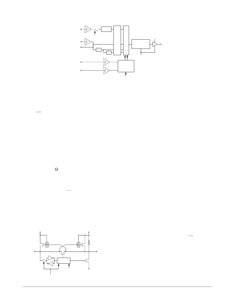
Figure 23. Clock Generator Functional Block
IO
RESET
SYNCLK
ASYCLKIN
INVOUT
CARDENABLE
S
L
S
SELECTOR
LATCH
SYNCHRO
LATCH
CRDVCC
CRDCLK
SEQ3
PROGRAM
2
LATCH
2
BIDIRECTIONAL LEVEL TRANSLATOR
This module (used on
IO/CRDIO
,
C4/CRDC4
,
C8/CRDC8
, see figure 24) adapts the signal voltage levels
of the I/O and control lines between the micro controller
(supplied by VBAT) and the smartcard (supplied by
CRDVCC)
When
CS
is low, with
CRDVCC
on, and start sequencing
completed, this module is transparent for the data, and acts
as if the card was directly connected to the reader
microcontroller. The core of the level shifter circuit defined
for the bidirectional
CRDIO
,
CRDC4
and
CRDC8
lines
consists of a NMOS switch which can be driven to the logic
low state from either side (microcontroller or card). If both
sides work in transmission mode with opposite phase, then
signal collision on the line is not avoidable. In this case, the
peak current is limited to a safe value for the integrated
circuit and the smartcard.
During high–to–low transitions, the NMOS transistor
impedance (T1=250 max.) is low enough to charge
parasitic capacitance, and have a high enough dv/dt. On low
to high transition, the NMOS transistor is not active above
a certain voltage, and an acceleration circuit is activated to
ensure a high dv/dt.
When the chip is disabled
(
CS
=
H
) with the voltage supply
CRDVCC
still active, the
IO
,
C4
and
C8
lines keep their last
logic state.
When the converter is off, a transistor forces the
CRDIO
,
CRDC4
and
CRDC8
lines to a low state, thus preventing
any unwanted voltage level to be applied to the data lines
when the card is not in use.
Figure 24. Bidirectional Translator Functional Block
VBAT
IO
(C4)
(C8)
18 K
CONTROL
LOGIC
SEQ1 (SEQ3)
T2
CRDIO
(CRDC4)
(CRDC8)
CRDGND
CARDENABLE
T1
CRDVCC
SECURITY FEATURES
The MC33560 has a number of unique security functions
to guarantee that no electrical damage will be caused to the
smartcard:
Battery supply minimum voltage threshold
Card supply undervoltage and overcurrent detection
with automatic shutdown
Card pin overvoltage clamp to CRDVCC
Card presence detector for ”clean” and fast shut–down
Consistent card signal sequencing at start–up and
power–down, according to ISO7816, even on error
conditions
Consistent clock signal, even when division ratio or
synchronization clock signal are changed ”on the fly” during
a card session (see figure 29)
Active pull–down on all card pins, including
CRDVCC
, when not in normal operating mode.
A current limiting function and an overtemperature
detector are limiting power dissipation.
ESD PROTECTION
Due to the nature of smartcards, the card interface pins
must absorb high ESD (Electro Static Discharge) energy
during card insertion. In addition, the control circuits
attached to these pins must safely withstand short circuits
and voltage transients during forced card extraction.
Therefore, the MC33560 features enhanced ESD
protection, current limitation and short circuit protection on
all smartcard interface pins, including
C4
and
C8
.
PARALLEL OPERATION
For applications where two or more MC33560 are used,
the digital control and data bus lines are common to all
MC33560. Only the chip select signal,
CS
, requires a
separate line for each interface.
While deselected, all communication pins except
CRDCLK
will keep their logical state on the card side, and
will go to high impedance mode on the microprocessor side.
Figure 33 shows a typical application of a dual card reader.
This arrangement was chosen only to illustrate the parallel
operation of two card interfaces in the same module. The
discrete capacitor components are necessary to provide low
相關PDF資料 |
PDF描述 |
|---|---|
| MC33560DW | Single Output LDO, 400mA, Fixed(3.0V), Low Noise, Fast Transient Response 8-MSOP -40 to 85 |
| MC33560DWR2 | Single Output LDO, 400mA, Fixed(3.0V), Low Noise, Fast Transient Response 8-MSOP -40 to 85 |
| MC33560DTBR2 | Power Management and Interface IC for Smartcard Readers and Couplers |
| MC33565 | Single Output LDO, 400mA, Fixed(3.0V), Low Noise, Fast Transient Response 5-SOT-23 -40 to 85 |
| MC33565D | Single Output LDO, 400mA, Fixed(3.0V), Low Noise, Fast Transient Response 5-SOT-23 -40 to 85 |
相關代理商/技術參數 |
參數描述 |
|---|---|
| MC33560DTBR2 | 功能描述:輸入/輸出控制器接口集成電路 3V/5V Smartcard RoHS:否 制造商:Silicon Labs 產品: 輸入/輸出端數量: 工作電源電壓: 最大工作溫度:+ 85 C 最小工作溫度:- 40 C 安裝風格:SMD/SMT 封裝 / 箱體:QFN-64 封裝:Tray |
| MC33560DTBR2G | 功能描述:輸入/輸出控制器接口集成電路 3V/5V Smartcard Power Management RoHS:否 制造商:Silicon Labs 產品: 輸入/輸出端數量: 工作電源電壓: 最大工作溫度:+ 85 C 最小工作溫度:- 40 C 安裝風格:SMD/SMT 封裝 / 箱體:QFN-64 封裝:Tray |
| MC33560DW | 功能描述:輸入/輸出控制器接口集成電路 3V/5V Smartcard RoHS:否 制造商:Silicon Labs 產品: 輸入/輸出端數量: 工作電源電壓: 最大工作溫度:+ 85 C 最小工作溫度:- 40 C 安裝風格:SMD/SMT 封裝 / 箱體:QFN-64 封裝:Tray |
| MC33560DWR2 | 功能描述:輸入/輸出控制器接口集成電路 3V/5V Smartcard RoHS:否 制造商:Silicon Labs 產品: 輸入/輸出端數量: 工作電源電壓: 最大工作溫度:+ 85 C 最小工作溫度:- 40 C 安裝風格:SMD/SMT 封裝 / 箱體:QFN-64 封裝:Tray |
| MC33560DWR2G | 功能描述:輸入/輸出控制器接口集成電路 3V/5V Smartcard Power Management RoHS:否 制造商:Silicon Labs 產品: 輸入/輸出端數量: 工作電源電壓: 最大工作溫度:+ 85 C 最小工作溫度:- 40 C 安裝風格:SMD/SMT 封裝 / 箱體:QFN-64 封裝:Tray |
發布緊急采購,3分鐘左右您將得到回復。