- 您現在的位置:買賣IC網 > PDF目錄371030 > MC34025P (MOTOROLA INC) Battery-Backup Supervisors for RAM Retention 8-MSOP -40 to 85 PDF資料下載
參數資料
| 型號: | MC34025P |
| 廠商: | MOTOROLA INC |
| 元件分類: | 穩壓器 |
| 英文描述: | Battery-Backup Supervisors for RAM Retention 8-MSOP -40 to 85 |
| 中文描述: | 2 A SWITCHING CONTROLLER, 1000 kHz SWITCHING FREQ-MAX, PDIP16 |
| 封裝: | PLASTIC, DIP-16 |
| 文件頁數: | 10/20頁 |
| 文件大小: | 516K |
| 代理商: | MC34025P |
MC34025 MC33025
10
MOTOROLA ANALOG IC DEVICE DATA
PIN FUNCTION DESCRIPTION
Pin No.
Function
Description
DIP/SOIC
1
Error Amp
Inverting
Input
This pin is usually used for feedback from the output of the power supply.
2
Error Amp
Noninverting
Input
This pin is used to provide a reference in which an error signal can be produced on the output of the
error amp. Usually this is connected to Vref, however an external reference can also
be used.
3
Error Amp
Output
This pin is provided for compensating the error amp for poles and zeros encountered in the power
supply system, mostly the output LC filter.
4
Clock
This is a bidirectional pin used for synchronization.
5
RT
CT
The value of RT sets the charge current through timing Capacitor, CT.
In conjunction with RT, the timing Capacitor sets the switching frequency. Because this part is a
push–pull output, each output runs at one–half the frequency set at this pin.
6
7
Ramp Input
For voltage mode operation this pin is connected to CT. For current mode operation this pin is
connected through a filter to the current sensing element.
8
Soft–Start
A capacitor at this pin sets the Soft–Start time.
9
Current
Limit/Shutdown
This pin has two functions. First, it provides cycle–by–cycle current limiting. Second, if the
current is excessive, this pin will reinitiate a Soft–Start cycle.
10
Ground
This pin is the ground for the control circuitry.
11
Output A
This is a high current totem pole output.
12
Power Ground
This is a separate power ground return that is connected back to the power source. It is used to
reduce the effects of switching transient noise on the control circuitry.
13
VC
This is a separate power source connection for the outputs that is connected back to the power source
input. With a separate power source connection, it can reduce the effects of switching transient noise
on the control circuitry.
14
Output B
This is a high current totem pole output.
15
VCC
Vref
This pin is the positive supply of the control IC.
16
This is a 5.1 V reference. It is usually connected to the noninverting input of the error amplifier.
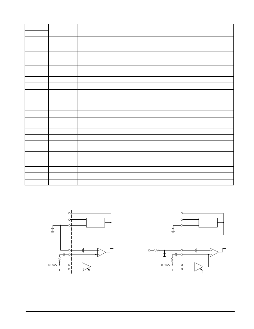
Output Voltage
Feedback Input
2
1
3
7
6
5
4
1.25 V
Oscillator
Vref
CT
Figure 21. Voltage Mode Operation
In voltage mode operation, the control range on the output of the Error
Amplifier from 0% to 90% duty cycle is from 2.25 V to 4.05 V.
Output Voltage
Feedback Input
2
1
3
7
6
5
4
1.25 V
Oscillator
Vref
CT
From Current
Sense Element
Figure 22. Current Mode Operation
In current mode control, an RC filter should be placed at the ramp input to filter
the leading edge spike caused by turn–on of a power MOSFET.
相關PDF資料 |
PDF描述 |
|---|---|
| MC3403 | Amplifiers and Comparators |
| MC34050P | Dual EIA-422/423 Transceivers |
| MC34050D | Dual EIA-422/423 Transceivers |
| MC34050 | Dual ELA-422/423 Transceivers |
| MC34051 | Dual ELA-422/423 Transceivers |
相關代理商/技術參數 |
參數描述 |
|---|---|
| MC34025PG | 功能描述:電流型 PWM 控制器 Dual Output Voltage or Current Mode PWM RoHS:否 制造商:Texas Instruments 開關頻率:27 KHz 上升時間: 下降時間: 工作電源電壓:6 V to 15 V 工作電源電流:1.5 mA 輸出端數量:1 最大工作溫度:+ 105 C 安裝風格:SMD/SMT 封裝 / 箱體:TSSOP-14 |
| MC3403 | 制造商:TI 制造商全稱:Texas Instruments 功能描述:QUADRUPLE LOW-POWER OPERATIONAL AMPLIFIERS |
| MC3403_06 | 制造商:ONSEMI 制造商全稱:ON Semiconductor 功能描述:Single Supply Quad Operational Amplifiers |
| MC3403D | 功能描述:運算放大器 - 運放 Quad Low Power RoHS:否 制造商:STMicroelectronics 通道數量:4 共模抑制比(最小值):63 dB 輸入補償電壓:1 mV 輸入偏流(最大值):10 pA 工作電源電壓:2.7 V to 5.5 V 安裝風格:SMD/SMT 封裝 / 箱體:QFN-16 轉換速度:0.89 V/us 關閉:No 輸出電流:55 mA 最大工作溫度:+ 125 C 封裝:Reel |
| MC3403D | 制造商:STMicroelectronics 功能描述:Operational Amplifier (Op-Amp) IC |
發布緊急采購,3分鐘左右您將得到回復。