- 您現(xiàn)在的位置:買賣IC網(wǎng) > PDF目錄371031 > MC34065P-H (MOTOROLA INC) Enhanced Product Single Voltage Detector 5-SC70 -40 to 125 PDF資料下載
參數(shù)資料
| 型號(hào): | MC34065P-H |
| 廠商: | MOTOROLA INC |
| 元件分類: | 穩(wěn)壓器 |
| 英文描述: | Enhanced Product Single Voltage Detector 5-SC70 -40 to 125 |
| 中文描述: | 0.4 A DUAL SWITCHING CONTROLLER, 500 kHz SWITCHING FREQ-MAX, PDIP16 |
| 封裝: | PLASTIC, DIP-16 |
| 文件頁數(shù): | 1/16頁 |
| 文件大小: | 419K |
| 代理商: | MC34065P-H |
SEMICONDUCTOR
TECHNICAL DATA
HIGH PERFORMANCE
DUAL CHANNEL CURRENT
MODE CONTROLLERS
ORDERING INFORMATION
PIN CONNECTIONS
Order this document by MC34065–H/D
P SUFFIX
PLASTIC PACKAGE
CASE 648
DW SUFFIX
PLASTIC PACKAGE
CASE 751G
(SO–16L)
Sync Input
CT
RT
Voltage Feedback 1
Compensation 1
Current Sense 1
Drive Output 1
Gnd
VCC
Vref
Drive Output 2 Enable
Voltage Feedback 2
Compensation 2
Current Sense 2
Drive Output 2
Drive Gnd
1
(Top View)
2
3
4
5
6
7
8
9
11
10
12
13
14
15
16
TA = –40
°
to +85
°
C
Device
Operating
Temperature Range
Package
SO–16L
MC34065DW–H
MC34065DW–L
MC34065P–H
TA = 0
°
to +70
°
C
MC34065P–L
MC33065DW–H
MC33065DW–L
MC33065P–H
MC33065P–L
Plastic DIP
SO–16L
Plastic DIP
1
MOTOROLA ANALOG IC DEVICE DATA
The MC34065–H,L series are high performance, fixed frequency, dual
current mode controllers. They are specifically designed for off–line and
dc–to–dc converter applications offering the designer a cost effective
solution with minimal external components. These integrated circuits feature
a unique oscillator for precise duty cycle limit and frequency control, a
temperature compensated reference, two high gain error amplifiers, two
current sensing comparators, Drive Output 2 Enable pin, and two high
current totem pole outputs ideally suited for driving power MOSFETs.
Also included are protective features consisting of input and reference
undervoltage lockouts each with hysteresis, cycle–by–cycle current limiting,
and a latch for single pulse metering of each output. These devices are
available in dual–in–line and surface mount packages.
The MC34065–H has UVLO thresholds of 14 V (on) and 10 V (off), ideally
suited for off–line converters. The MC34065–L is tailored for lower voltage
applications having UVLO thresholds of 8.4 V (on) and 7.8 V (off).
Unique Oscillator for Precise Duty Cycle Limit and Frequency Control
Current Mode Operation to 500 kHz
Automatic Feed Forward Compensation
Separate Latching PWMs for Cycle–By–Cycle Current Limiting
Internally Trimmed Reference with Undervoltage Lockout
Drive Output 2 Enable Pin
Two High Current Totem Pole Outputs
Input Undervoltage Lockout with Hysteresis
Low Startup and Operating Current
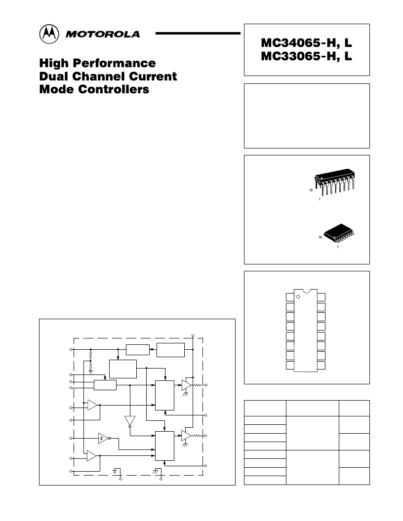
Representative Block Diagram
+
–
+
–
Error
Amp 1
Vref
Sync Input
RT
CT
Voltage
Feedback 1
Compensation 1
Drive Output
2
Enable
Voltage
Feedback 2
Compensation 2
15
1
5
13
12
14
4
2
3
7
6
10
11
Drive Output 1
Current Sense 1
Drive Output 2
Current Sense 2
VCC
16
Gnd
8
Drive Gnd
9
Error
Amp 2
Oscillator
UndVref
Lockout
5.0V
Reference
UndVCC
Lockout
Latching
PWM 1
Latching
PWM 2
R
R
Motorola, Inc. 1996
Rev 0
相關(guān)PDF資料 |
PDF描述 |
|---|---|
| MC34066DW | HIGH PERFORMANCE RESONANT MODE CONTROLLERS |
| MC33066DW | HIGH PERFORMANCE RESONANT MODE CONTROLLERS |
| MC33066P | HIGH PERFORMANCE RESONANT MODE CONTROLLERS |
| MC34066P | Enhanced Product Single Voltage Detectors 5-SC70 -55 to 125 |
| MC33066 | HIGH PERFORMANCE RESONANT MODE CONTROLLERS |
相關(guān)代理商/技術(shù)參數(shù) |
參數(shù)描述 |
|---|---|
| MC34065P-L | 制造商:MOTOROLA 制造商全稱:Motorola, Inc 功能描述:HIGH PERFORMANCE DUAL CHANNEL CURRENT MODE CONTROLLERS |
| MC34066 | 制造商:MOTOROLA 制造商全稱:Motorola, Inc 功能描述:HIGH PERFORMANCE RESONANT MODE CONTROLLERS |
| MC34066DW | 制造商:MOTOROLA 制造商全稱:Motorola, Inc 功能描述:HIGH PERFORMANCE RESONANT MODE CONTROLLERS |
| MC34066P | 制造商:MOTOROLA 制造商全稱:Motorola, Inc 功能描述:High Performance Resonant Mode Controllers |
| MC34067 | 制造商:ONSEMI 制造商全稱:ON Semiconductor 功能描述:High Performance Resonant Mode Controllers |
發(fā)布緊急采購(gòu),3分鐘左右您將得到回復(fù)。