- 您現在的位置:買賣IC網 > PDF目錄371031 > MC34066 (Motorola, Inc.) HIGH PERFORMANCE RESONANT MODE CONTROLLERS PDF資料下載
參數資料
| 型號: | MC34066 |
| 廠商: | Motorola, Inc. |
| 英文描述: | HIGH PERFORMANCE RESONANT MODE CONTROLLERS |
| 中文描述: | 高性能諧振模式控制器 |
| 文件頁數: | 2/12頁 |
| 文件大小: | 168K |
| 代理商: | MC34066 |
MC34066 MC33066
2
MOTOROLA ANALOG IC DEVICE DATA
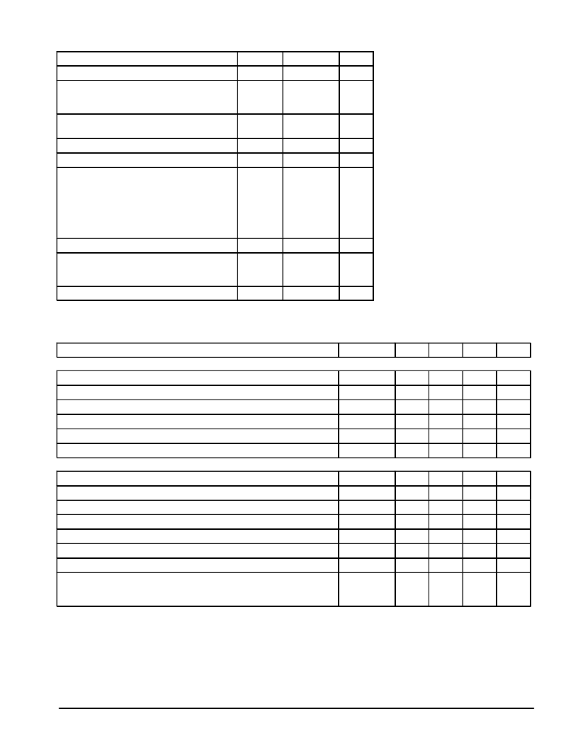
MAXIMUM RATINGS
Rating
Symbol
Value
Unit
Power Input Supply Voltage
VCC
IO
20
V
Drive Output Current, Source or Sink (Note 1)
Continuous
Pulsed (0.5
μ
s, 25% Duty Cycle)
0.3
1.5
A
Error Amplifier, Fault, One–Shot, Oscillator, and
Soft–Start Inputs
Vin
–1.0 to +6.0
V
UVLO Adjust Input
Vin(UVLO)
Idchg
–1.0 to VCC
20
V
Soft–Start Discharge Current
mA
Power Dissipation and Thermal Characteristics
DW Suffix Package, Case 751G
Maximum Power Dissipation @ TA = 25
°
C
Thermal Resistance, Junction–to–Air
P Suffix Package, Case 648
Maximum Power Dissipation @ TA = 25
°
C
Thermal Resistance, Junction–to–Air
PD
R
θ
JA
PD
R
θ
JA
TJ
TA
862
145
1.25
100
mW
°
C/W
W
°
C/W
Operating Junction Temperature
+150
°
C
Operating Ambient Temperature
MC34066
MC33066
0 to +70
–40 to +85
°
C
Storage Temperature Range
Tstg
–65 to +150
°
C
ELECTRICAL CHARACTERISTICS
(VCC = 12 V [Note 2], ROSC = 95.3 k, RDT = 0
, RVFO = 5.62 k, COSC = 300 pF, RT = 14.3 k,
CT = 300 pF, CL = 1.0 nF, for typical values TA = 25
°
C, for min/max values TA is the operating ambient temperature range that applies
[Note 3], unless otherwise noted.)
Characteristics
Symbol
Min
Typ
Max
Unit
REFERENCE SECTION
Reference Output Voltage (IO = 0 mA, TA = 25
°
C)
Line Regulation (VCC = 10 V to 18 V)
Load Regulation (IO = 0 mA to 10 mA)
Total Output Variation over Line, Load, and Temperature
Vref
Regline
Regload
Vref
IO
Vth
5.0
5.1
5.2
V
–
1.0
20
mV
–
1.0
20
mV
4.9
–
5.3
mV
Output Short Circuit Current
25
100
190
mA
Reference Undervoltage Lockout Threshold
3.8
4.3
4.8
V
ERROR AMPLIFIER
Input Offset Voltage (VCM = 1.5 V)
Input Bias Current (VCM = 1.5 V)
Input Offset Current (VCM = 1.5 V)
Open Loop Voltage Gain (VCM = 1.5 V, VO = 2.0 V)
Gain Bandwidth Product (f = 100 kHz)
VIO
IIB
IIO
AVOL
GBW
–
1.0
10
mV
–
0.2
1.0
μ
A
–
0
0.5
μ
A
70
100
–
dB
2.5
4.2
–
MHz
Input Common Mode Rejection Ratio (VCM = 1.5 V to 5.0 V)
Power Supply Rejection Ratio (VCC = 10 V to 18 V, f = 120 Hz)
Output Voltage Swing
High State with Respect to Pin 3 (ISource = 2.0 mA)
Low State with Respect to Ground (ISink = 1.0 mA)
CMRR
70
95
–
dB
PSRR
80
100
–
dB
VOH
VOL
2.3
–
2.7
0.4
3.1
0.6
V
NOTES:
1.Maximum package power dissipation limits must be observed.
2.Adjust VCC above the Startup threshold before setting to 12 V.
3.Low duty cycle pulse techniques are used during test to maintain junction temperature as close to ambient as possible.
Tlow= 0
°
C for MC34066
Thigh=
–40
°
C for MC33066
Thigh=
+70
°
C for MC34066
+85
°
C for MC33066
相關PDF資料 |
PDF描述 |
|---|---|
| MC34080 | Low Quiescent Current, Programmable-Delay Supervisory Circuit 6-SOT-23 -40 to 125 |
| MC34081BD | Low Quiescent Current, Programmable-Delay Supervisory Circuit 6-SOT-23 -40 to 125 |
| MC34081BP | Low Quiescent Current, Programmable-Delay Supervisory Circuit 6-SON -40 to 125 |
| MC34080 | Low Quiescent Current, Programmable-Delay Supervisory Circuit 6-SOT-23 -40 to 125 |
| MC34082P | Low Quiescent Current, Programmable-Delay Supervisory Circuit 6-SOT-23 -40 to 125 |
相關代理商/技術參數 |
參數描述 |
|---|---|
| MC34066DW | 制造商:MOTOROLA 制造商全稱:Motorola, Inc 功能描述:HIGH PERFORMANCE RESONANT MODE CONTROLLERS |
| MC34066P | 制造商:MOTOROLA 制造商全稱:Motorola, Inc 功能描述:High Performance Resonant Mode Controllers |
| MC34067 | 制造商:ONSEMI 制造商全稱:ON Semiconductor 功能描述:High Performance Resonant Mode Controllers |
| MC34067_05 | 制造商:ONSEMI 制造商全稱:ON Semiconductor 功能描述:High Performance Resonant Mode Controllers |
| MC34067_09 | 制造商:ONSEMI 制造商全稱:ON Semiconductor 功能描述:High Performance Resonant Mode Controllers |
發布緊急采購,3分鐘左右您將得到回復。