- 您現在的位置:買賣IC網 > PDF目錄371031 > MC34081AD (MOTOROLA INC) Low Quiescent Current, Programmable-Delay Supervisory Circuit 6-SOT-23 -40 to 125 PDF資料下載
參數資料
| 型號: | MC34081AD |
| 廠商: | MOTOROLA INC |
| 元件分類: | 運動控制電子 |
| 英文描述: | Low Quiescent Current, Programmable-Delay Supervisory Circuit 6-SOT-23 -40 to 125 |
| 中文描述: | OP-AMP, 2500 uV OFFSET-MAX, 8 MHz BAND WIDTH, PDSO8 |
| 封裝: | PLASTIC, SO-8 |
| 文件頁數: | 1/16頁 |
| 文件大小: | 282K |
| 代理商: | MC34081AD |
$"%
HIGH PERFORMANCE
JFET INPUT
OPERATIONAL AMPLIFIERS
Order this document by MC34080/D
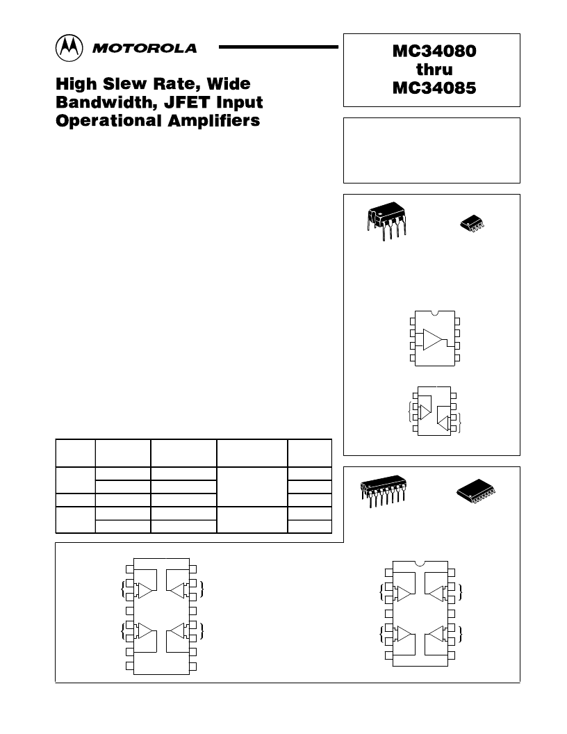
D SUFFIX
PLASTIC PACKAGE
CASE 751
(SO–8)
P SUFFIX
PLASTIC PACKAGE
CASE 626
DW SUFFIX
PLASTIC PACKAGE
CASE 751G
(SO–16L)
P SUFFIX
PLASTIC PACKAGE
CASE 646
PIN CONNECTIONS
PIN CONNECTIONS
(Single, Top View)
(Dual, Top View)
(Quad, Top View)
4
2
3
1
4
2
3
1
–
Offset Null
Noninv. Input
VEE
Inv. Input
VEE
Inputs 1
Output 1
NC
VCC
Output
Offset Null
Inputs 2
Output 2
VCC
1
2
3
4
8
7
6
5
+
1
2
3
4
8
7
6
5
–
+
–
+
Inputs 1
Output 1
VCC
Inputs 2
Output 2
Inputs 1
Output 1
VCC
Inputs 2
Output 2
NC
Output 4
Inputs 4
VEE
Inputs 3
Output 3
Output 4
Inputs 4
VEE
Inputs 3
Output 3
NC
1
2
3
4
5
6
7
10
11
12
13
14
15
16
8
9
1
2
3
4
5
6
7
8
9
10
11
12
13
14
–
+
–
+
+
–
+
–
–
+
–
+
+
–
+
–
1
8
1
8
14
1
16
1
MOTOROLA ANALOG IC DEVICE DATA
t
& $
&$ !%$
!"$ !"#
These devices are a new generation of high speed JFET input monolithic
operational amplifiers. Innovative design concepts along with JFET
technology provide wide gain bandwidth product and high slew rate.
Well–matched JFET input devices and advanced trim techniques ensure low
input offset errors and bias currents. The all NPN output stage features large
output voltage swing, no deadband crossover distortion, high capacitive
drive capability, excellent phase and gain margins, low open loop output
impedance, and symmetrical source/sink AC frequency response.
This series of devices is available in fully compensated or
decompensated (AVCL
≤
2) and is specified over a commercial temperature
range. They are pin compatible with existing Industry standard operational
amplifiers, and allow the designer to easily upgrade the performance of
existing designs.
Wide Gain Bandwidth: 8.0 MHz for Fully Compensated Devices
Wide Gain Bandwidth:
16 MHz for Decompensated Devices
High Slew Rate: 25 V/
μ
s for Fully Compensated Devices
High Slew Rate:
50 V/
μ
s for Decompensated Devices
High Input Impedance: 1012
Input Offset Voltage: 0.5 mV Maximum (Single Amplifier)
Large Output Voltage Swing: –14.7 V to +14 V for
Large Output Voltage Swing:
VCC/VEE =
±
15 V
Low Open Loop Output Impedance: 30
@ 1.0 MHz
Low THD Distortion: 0.01%
Excellent Phase/Gain Margins: 55
°
/7.6 dB for Fully Compensated
Devices
ORDERING INFORMATION
Op Amp
Function
Fully
Compen-
sated
AVCL
≥
2
Compensated
Operating
Temperature
Range
Package
Single
MC34081BD
MC34080BD
TA = 0
to +70
°
°
C
SO–8
MC34081BP
MC34080BP
Plastic DIP
Dual
MC34082P
MC34083BP
Plastic DIP
Quad
MC34084DW
MC34085BDW
TA= 0
TA = 0
°
to +70
°
C
SO–16L
MC34084P
MC34085BP
Plastic DIP
Motorola, Inc. 1996
Rev 0
相關PDF資料 |
PDF描述 |
|---|---|
| MC34081AP | Low Quiescent Current, Programmable-Delay Supervisory Circuit 6-SOT-23 -40 to 125 |
| MC34081BD | Low Quiescent Current, Programmable-Delay Supervisory Circuit 6-SON -40 to 125 |
| MC34081BP | Low Quiescent Current, Programmable-Delay Supervisory Circuit 6-SON -40 to 125 |
| MC34081D | Low Quiescent Current, Programmable-Delay Supervisory Circuit 6-SOT-23 -40 to 125 |
| MC34081P | Low Quiescent Current, Programmable-Delay Supervisory Circuit 6-SOT-23 -40 to 125 |
相關代理商/技術參數 |
參數描述 |
|---|---|
| MC34081AP | 制造商:MOTOROLA 制造商全稱:Motorola, Inc 功能描述:HIGH SLEW RATE, WIDE BANDWIDTH, JEFT INPUT OPERATIONAL AMPLIFIERS |
| MC34081B | 制造商:MOTOROLA 制造商全稱:Motorola, Inc 功能描述:Amplifiers and Comparators |
| MC34081BD | 制造商:Rochester Electronics LLC 功能描述:- Bulk |
| MC34081BDR2 | 制造商:Motorola Inc 功能描述: |
| MC34081BP | 制造商:Rochester Electronics LLC 功能描述:- Bulk |
發布緊急采購,3分鐘左右您將得到回復。