- 您現在的位置:買賣IC網 > PDF目錄371032 > MC34119DTB (MOTOROLA INC) LOW POWER AUDIO AMPLIFIER PDF資料下載
參數資料
| 型號: | MC34119DTB |
| 廠商: | MOTOROLA INC |
| 元件分類: | 音頻/視頻放大 |
| 英文描述: | LOW POWER AUDIO AMPLIFIER |
| 中文描述: | 0.4 W, 1 CHANNEL, AUDIO AMPLIFIER, PDSO8 |
| 封裝: | PLASTIC, TSSOP-8 |
| 文件頁數: | 4/12頁 |
| 文件大小: | 264K |
| 代理商: | MC34119DTB |
MC34119
4
MOTOROLA ANALOG IC DEVICE DATA
DESIGN GUIDELINES
General
The MC34119 is a low power audio amplifier capable of
low voltage operation (VCC = 2.0 V minimum) such as that
encountered in line–powered speakerphones. The circuit
provides a differential output (VO1–VO2) to the speaker to
maximize the available voltage swing at low voltages. The
differential gain is set by two external resistors. Pins FC1 and
FC2 allow controlling the amount of power supply and noise
rejection, as well as providing alternate inputs to the
amplifiers. The CD pin permits powering down the IC for
muting purposes and to conserve power.
Amplifiers
Referring to the block diagram, the internal configuration
consists of two identical operational amplifiers. Amplifier #1
has an open loop gain of
≥
80 dB (at f
≤
100 Hz), and the
closed loop gain is set by external resistor Rf and Ri. The
amplifier is unity gain stable, and has a unity gain frequency
of approximately 1.5 MHz. In order to adequately cover the
telephone voice band (300 Hz to 3400 Hz), a maximum
closed loop gain of 46 is recommended. Amplifier #2 is
internally set to a gain of – 1.0 (0 dB).
The outputs of both amplifiers are capable of sourcing and
sinking a peak current of 200 mA. The outputs can typically
swing to within
≈
0.4 V above ground, and to within
≈
1.3 V
below VCC, at the maximum current. See Figures 18 and 19
for VOH and VOL curves.
The output dc offset voltage (VO1–VO2) is primarily a
function of the feedback resistor (Rf), and secondarily due to
the amplifiers’ input offset voltages. The input offset voltage
of the two amplifiers will generally be similar for a particular
IC, and therefore nearly cancel each other at the outputs.
Amplifier #1’s bias current, however, flows out of Vin (Pin 4)
and through Rf, forcing VO1 to shift negative by an amount
equal to [Rf
×
IIB]. VO2 is shifted positive an equal amount.
The output offset voltage, specified in the Electrical
Characteristics, is measured with the feedback resistor
shown in the Typical Application Circuit, and therefore takes
into account the bias current as well as internal offset
voltages of the amplifiers. The bias current is constant with
respect to VCC.
FC1 and FC2
Power supply rejection is provided by the capacitors (C1
and C2 in the Typical Application Circuit) at FC1 and FC2. C2
is somewhat dominant at low frequencies, while C1 is
dominant at high frequencies, as shown in the graphs of
Figures 4 to 7. The required values of C1 and C2 depend on
the conditions of each application. A line powered
speakerphone, for example, will require more filtering than a
circuit powered by a well regulated power supply. The
amount of rejection is a function of the capacitors, and the
equivalent impedance looking into FC1 and FC2 (listed in the
Electrical Characteristics as RFC1 and RFC2).
In addition to providing filtering, C1 and C2 also affect the
turn–on time of the circuit at power–up, since the two
capacitors must charge up through the internal 50 k and
125 k
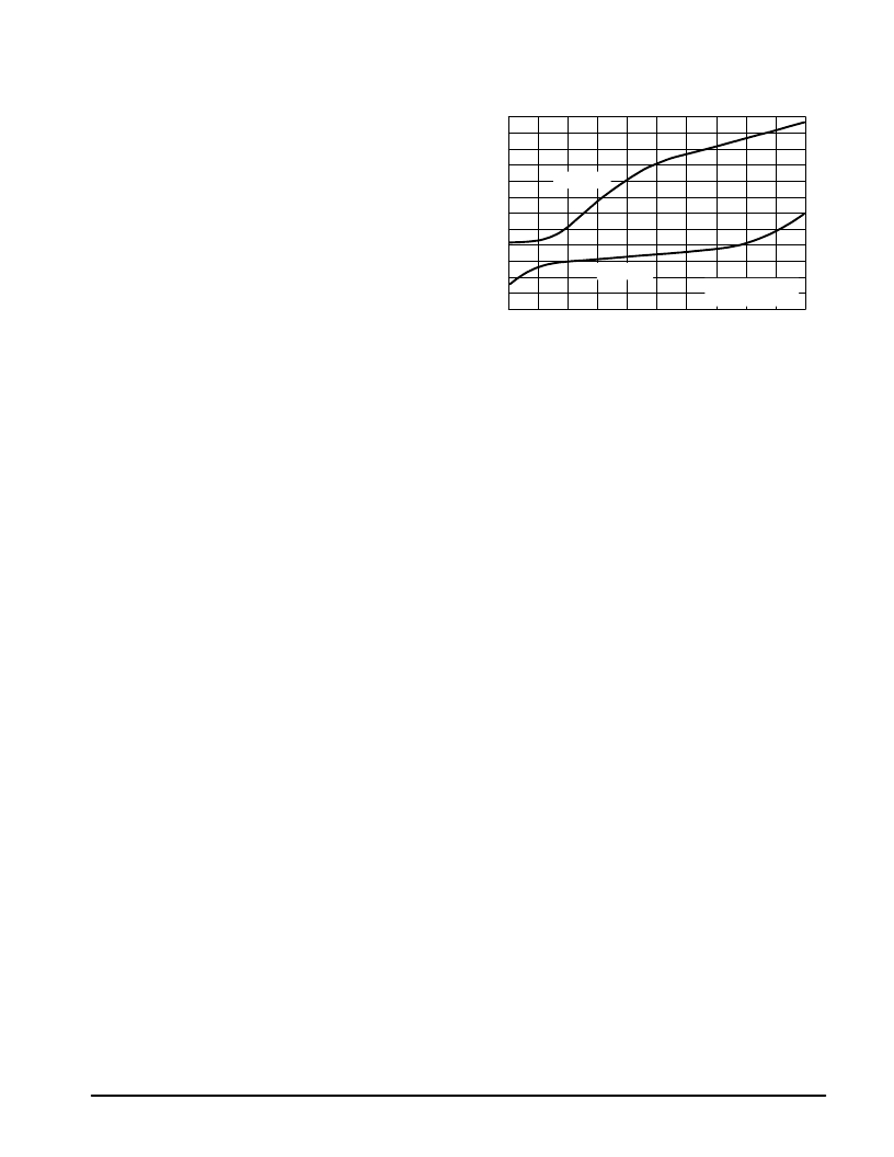
resistors. The graph of Figure 1 indicates the
turn–on time upon application of VCC of +6.0 V. The turn–on
time is
≈
60% longer for VCC = 3.0 V, and
≈
20% less for
VCC = 9.0 V. Turn–off time is <10
μ
s upon removal of VCC.
t
C2, CAPACITANCE (
μ
F)
Figure 1. Turn–On Time versus C1, C2 at Power–On
360
300
240
180
120
60
0
0
2.0
4.0
6.0
8.0
10
C1 = 5.0
μ
F
C1 = 1.0
μ
F
VCC switching from
0 V to 6.0 V
Chip Disable
The Chip Disable (Pin 1) can be used to power down the
IC to conserve power, or for muting, or both. When at a Logic
“0” (0 V to 0.8 V), the MC34119 is enabled for normal
operation. When Pin 1 is at a Logic “1” (2.0 V to VCC V), the
IC is disabled. If Pin 1 is open, that is equivalent to a Logic
“0,” although good design practice dictates that an input
should never be left open. Input impedance at Pin 1 is a
nominal 90 k
. The power supply current (when disabled) is
shown in Figure 15.
Muting, defined as the change in differential gain from
normal operation to muted operation, is in excess of 70 dB.
The turn–off time of the audio output, from the application of
the CD signal, is <2.0
μ
s, and turn on–time is 12 ms–15 ms.
Both times are independent of C1, C2, and VCC.
When the MC34119 is disabled, the voltages at FC1 and
FC2 do not change as they are powered from VCC. The
outputs, VO1 and VO2, change to a high impedance condition,
removing the signal from the speaker. If signals from other
sources are to be applied to the outputs (while disabled), they
must be within the range of VCC and Ground.
Power Dissipation
Figures 8 to 10 indicate the device dissipation (within the
IC) for various combinations of VCC, RL, and load power. The
maximum power which can safely be dissipated within the
MC34119 is found from the following equation:
PD = (140
°
C – TA)/
θ
JA
where TA is the ambient temperature; and
θ
JA is the package
thermal resistance (100
°
C/W for the standard DIP package,
and 180
°
C/W for the surface mount package.)
The power dissipated within the MC34119, in a given
application, is found from the following equation:
PD = (VCC x ICC) + (IRMS x VCC) – (RL x IRMS2)
where ICC is obtained from Figure 15; and IRMS is the RMS
current at the load; and RL is the load resistance.
Figures 8 to 10, along with Figures 11 to 13 (distortion
curves), and a peak working load current of
±
200 mA, define
the operating range for the MC34119. The operating range is
further defined in terms of allowable load power in Figure 14
for loads of 8.0
, 16
and 32
. The left (ascending) portion
相關PDF資料 |
PDF描述 |
|---|---|
| MC34119 | ECONOLINE: RSZ/P - 1kVDC |
| MC34119D | LOW POWER AUDIO AMPLIFIER |
| MC34129 | HIGH PERFORMANCE CURRENT MODE CONTROLLERS |
| MC33129D | HIGH PERFORMANCE CURRENT MODE CONTROLLERS |
| MC33129P | HIGH PERFORMANCE CURRENT MODE CONTROLLERS |
相關代理商/技術參數 |
參數描述 |
|---|---|
| MC34119DTBR2 | 功能描述:IC AMP AUDIO 4W MONO AB 8TSSOP RoHS:否 類別:集成電路 (IC) >> 線性 - 音頻放大器 系列:- 產品培訓模塊:Lead (SnPb) Finish for COTS Obsolescence Mitigation Program 標準包裝:2,500 系列:DirectDrive® 類型:H 類 輸出類型:耳機,2-通道(立體聲) 在某負載時最大輸出功率 x 通道數量:35mW x 2 @ 16 歐姆 電源電壓:1.62 V ~ 1.98 V 特點:I²C,麥克風,靜音,短路保護,音量控制 安裝類型:表面貼裝 供應商設備封裝:25-WLP(2.09x2.09) 封裝/外殼:25-WFBGA,WLCSP 包裝:帶卷 (TR) |
| MC34119EC | 制造商:Rochester Electronics LLC 功能描述: 制造商:Freescale Semiconductor 功能描述: |
| MC34119EF | 制造商:Freescale Semiconductor 功能描述:LOW POWER AUDIO AMPLIFIER |
| MC34119G-D08-T | 制造商:UTC-IC 制造商全稱:UTC-IC 功能描述:LOW POWER AUDIO AMPLIFIER |
| MC34119G-P08-R | 制造商:UTC-IC 制造商全稱:UTC-IC 功能描述:LOW POWER AUDIO AMPLIFIER |
發布緊急采購,3分鐘左右您將得到回復。