- 您現在的位置:買賣IC網 > PDF目錄371034 > MC34270FB (MOTOROLA INC) Single Output LDO, 250mA, Fixed(3.0V), Low Noise, Fast Transient Response 5-SOT-23 -40 to 85 PDF資料下載
參數資料
| 型號: | MC34270FB |
| 廠商: | MOTOROLA INC |
| 元件分類: | 穩壓器 |
| 英文描述: | Single Output LDO, 250mA, Fixed(3.0V), Low Noise, Fast Transient Response 5-SOT-23 -40 to 85 |
| 中文描述: | 0.5 A DUAL SWITCHING CONTROLLER, 700 kHz SWITCHING FREQ-MAX, PQFP32 |
| 封裝: | PLASTIC, QFP-32 |
| 文件頁數: | 6/12頁 |
| 文件大小: | 364K |
| 代理商: | MC34270FB |
MC34270 MC34271
6
MOTOROLA ANALOG IC DEVICE DATA
VDD LEVEL (V)
0
0
1000
R
F
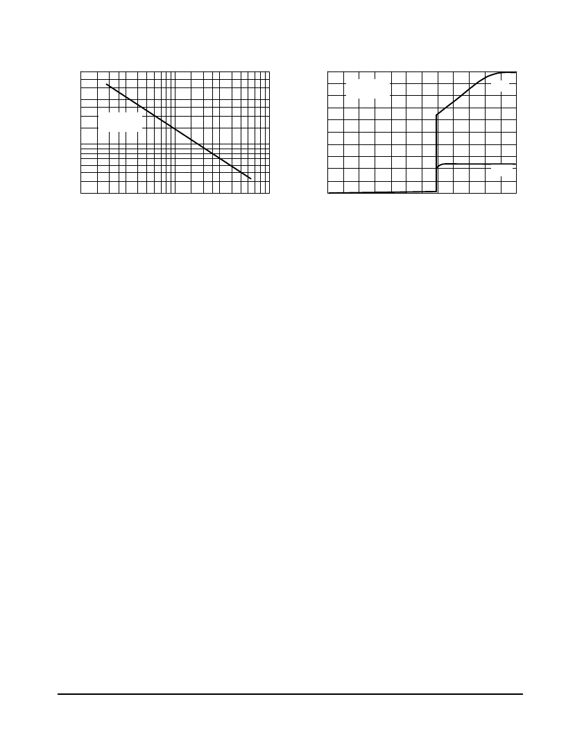
Figure 9. Frequency versus Timing
TIMING RESISTANCE (k
, s)
Figure 10. VA, Vref versus VDD
100
10
5.0
4.0
3.0
2.0
1.0
0
100
1000
1.0
2.0
3.0
4.0
5.0
6.0
VDD = 6.0 V
TA = 25
°
C
RT = 169 k
TA = 25
°
C
VA
Vref
OPERATING DESCRIPTION
The MC34270 and MC34271 series are monolithic, fixed
frequency power switching regulators specifically designed
for dc to dc converter and battery powered applications.
These devices operate as fixed frequency, voltage mode
regulators containing all the active functions required to
directly implement step–up, step–down and voltage inverting
converters with a minimum number of external components.
Potential markets include battery powered, handheld,
automotive, computer, industrial and cost sensitive consumer
products. A description of each section is given below with
the representative block diagram shown in Figure 9.
Oscillator
The oscillator frequency is programmed by resistor RT.
The charge to discharge ratio is controlled to yield a 95%
maximum duty cycle at the switch outputs. During the fall
time of the internal sawtooth waveform, the oscillator
generates an internal blanking pulse that holds the inverting
input of the AND gates high, disabling the output switching
MOSFETs. The internal sawtooth waveform has a nominal
peak voltage of 3.3 V and a valley voltage of 1.7 V.
Pulse Width Modulators
Both pulse width modulators consist of a comparator with
the oscillator ramp voltage applied to the noninverting input,
while the error amplifier output is applied to the inverting
input. A third input to the comparator has a 0.5 mA typical
current source that can be used to implement soft start.
Output switch conduction is initiated when the ramp
waveform is discharged to the valley voltage. As the ramp
voltage increases to a voltage that exceeds the error
amplifier output, the latch resets, terminating output
MOSFET conduction for the duration of the oscillator ramp.
This PWM/latch combination prevents multiple output pulses
during a given oscillator cycle.
Each PWM circuit is enabled by a logic input. When
disabled, the entire block is turned off, drawing only leakage
current from the power source. Shared circuits, like the
reference and oscillator, can be activated by either EN1
or EN2.
Circuit #1 has an ELD output which may be used to drive
an LCD or backlight. Its output frequency is the oscillator
frequency divided by 1024.
Error Amplifiers and Reference
Each error amplifier is provided with access to both
inverting and noninverting inputs, and the output. The Error
Amplifiers’ Common Mode Input Range is 0 to 2.5 V. The
amplifiers have a minimum dc voltage gain of 60 dB. The
1.25 V reference has an accuracy of
±
4.0% at room
temperature.
External loop compensation is required for converter
stability. A simple low–pass filter is formed by connecting a
resistive divider from the output to the error amplifier
inverting input, and a series resistor–capacitor from the error
amplifier output also to the to the inverting input. The step
down converter is easiest to compensate for stability. The
step–up and voltage inverting configurations, when operated
as continuous conduction boost or flyback converters, are
more difficult to compensate, and may require a lower loop
design bandwidth.
MOSFET Switch Outputs
The output MOSFETs are designed to switch a maximum
of 60 V, with a peak drain current capability of 500 mA. In
circuit #1 an additional DRV1 output is provided for
interfacing with an external MOSFET.The gates of the
MOSFETs are held low when the circuit is disabled.
Auxiliary Output Voltages
Output voltages V0 through V4 are provided for use as
references or bias voltages. V0 is the circuit #2 output
voltage, when an internal FET switch is activated. The other
auxiliary output voltages are proportional to VB. The
amplifiers for V1 and V2 are powered from V0, while the
amplifiers for V3 and V4 are powered from VDD.
相關PDF資料 |
PDF描述 |
|---|---|
| MC3447 | BIDIRECTIONAL INSTRUMENTATION BUS(GPIB) TRANSCEIVER |
| MC3447P3 | BIDIRECTIONAL INSTRUMENTATION BUS(GPIB) TRANSCEIVER |
| MC3447P | BIDIRECTIONAL INSTRUMENTATION BUS(GPIB) TRANSCEIVER |
| MC3447L | BIDIRECTIONAL INSTRUMENTATION BUS(GPIB) TRANSCEIVER |
| MC3448AL | QUAD THREE-STATE BUS TRANSCEIVER WITH TERMINATION NETWORKS |
相關代理商/技術參數 |
參數描述 |
|---|---|
| MC34271FB | 制造商:Rochester Electronics LLC 功能描述:- Bulk |
| MC34280FTB | 制造商:ON Semiconductor 功能描述: |
| MC3430 | 制造商:mCube 功能描述: |
| MC3430P | 制造商:Motorola Inc 功能描述: |
| MC34311 | 制造商:SPC Multicomp 功能描述:HEADER R/ANGLE 2WAY 制造商:SPC Multicomp 功能描述:HEADER, R/ANGLE, 2WAY 制造商:SPC Multicomp 功能描述:WIRE-BOARD CONNECTOR, RCPT, 2POS, 4.2MM; Series:2261(5561); Pitch Spacing:4.2mm; Contact Termination:Through Hole Right Angle; No. of Contacts:2; No. of Rows:2; Connector Mounting:PCB; Gender:Receptacle; Contact Material:Copper Alloy;RoHS Compliant: Yes |
發布緊急采購,3分鐘左右您將得到回復。