- 您現在的位置:買賣IC網 > PDF目錄371035 > MC44144D (MOTOROLA INC) SUBCARRIER PHASE-LOCKED LOOP PDF資料下載
參數資料
| 型號: | MC44144D |
| 廠商: | MOTOROLA INC |
| 元件分類: | XO, clock |
| 英文描述: | SUBCARRIER PHASE-LOCKED LOOP |
| 中文描述: | PHASE LOCKED LOOP, PDSO8 |
| 封裝: | PLASTIC, SO-8 |
| 文件頁數: | 4/8頁 |
| 文件大小: | 117K |
| 代理商: | MC44144D |
MC44144
4
MOTOROLA ANALOG IC DEVICE DATA
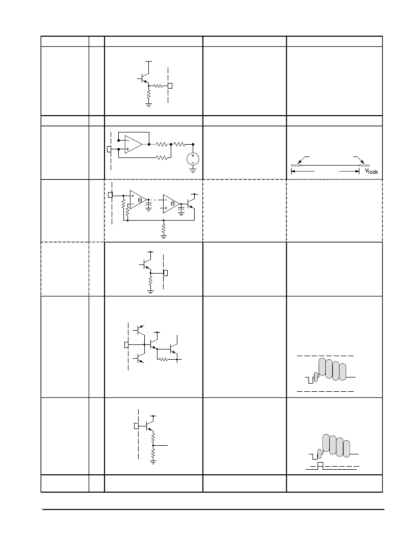
PIN FUNCTION DESCRIPTION
Name
Pin
Representative Circuitry
Description
Expected Waveforms
Subcarrier
Output
1
5.0k
200
VCC
Subcarrier Output. A
phase–locked reference of the
PAL or NTSC color burst is
output at this pin.
A 300 mVpp square wave is output.
Some high frequency content is
present.
Ground
2
Circuit Ground
Phase
Detector
Output
3
1.0k
31k
33k
2.5V
The error current from the
phase detector is output at this
pin. A filter circuit should be
connected at this pin.
A beat waveform, showing both
horizontal period and half the
subcarrier period, is present.
Line Period
1/2 Subcarrier Period
4X Sub Xtal
4
gm
2.0k
400
VCC
Vref
gm
Crystal Oscillator Pin. A 4X
subcarrier parallel resonant
crystal, in series with a 5.0 to
25 pF trimmer capacitor
provides the resonant element
for the Voltage Controlled
Crystal Oscillator (VCXO).
Approximately 40 mVpp. A scope
probe will disturb the frequency of
oscillation.
4X Subcarrier
Output (or
Black Burst)
5
5.0k
VCC
Buffered output from the 4X
voltage controlled oscillator.
The sinusoidal 4Xfsc oscillator output
is available at this pin.
The output is nominally:
525 mVpp for NTSC,
425 mVpp for PAL.
Composite
Video Input
(Black Burst,
Continuous
Wave, or
Composite
Chroma
can also be
applied)
6
22k
VCC
Composite Video Input. Color
burst from the video present at
this pin is used as a reference
to phase lock the VCXO.
Positive or negative video may
be used.
Composite video should be applied
at this pin. The color burst
amplitude of the input video should
be at least 50 mV, but no more than
1000 mV. The waveform at this pin
should not exceed ground or VCC.
VCC
GND
2.6V
Burst Gate
Input
7
VCC
22k
22k
Input for the phase detector
gate pulse. TTL compatible.
The threshold is nominally
2.6V.
A positive going gate pulse should
be applied at this pin. The Burst Gate
input should envelope the color
burst.
Pin 7
2.2V
Pin 6
VCC
8
Power Supply Pin. 5.0 Vdc
should be applied at this pin.
相關PDF資料 |
PDF描述 |
|---|---|
| MC44144 | SUBCARRIER PHASE-LOCKED LOOP |
| MC44144P | SUBCARRIER PHASE-LOCKED LOOP |
| MC44145D | PIXEL CLOCK GENERATOR/ SYNC SEPARATOR |
| MC44251 | Triple 8-Bit Video ADC Three-State Outputs |
| MC44251FN | Triple 8-Bit Video ADC Three-State Outputs |
相關代理商/技術參數 |
參數描述 |
|---|---|
| MC44144D1 | 制造商:Motorola Inc 功能描述: |
| MC44144P | 制造商:MOTOROLA 制造商全稱:Motorola, Inc 功能描述:SUBCARRIER PHASE-LOCKED LOOP |
| MC44145 | 制造商:MOTOROLA 制造商全稱:Motorola, Inc 功能描述:PIXEL CLOCK GENERATOR / SYNC SEPARATOR |
| MC44145D | 制造商:MOTOROLA 制造商全稱:Motorola, Inc 功能描述:PIXEL CLOCK GENERATOR/ SYNC SEPARATOR |
| MC4418 | 制造商:SHENZHENFREESCALE 制造商全稱:ShenZhen FreesCale Electronics. Co., Ltd 功能描述:N-Channel 30-V (D-S) MOSFET High performance trench technology |
發布緊急采購,3分鐘左右您將得到回復。