- 您現(xiàn)在的位置:買賣IC網(wǎng) > PDF目錄371035 > MC44251FN (MOTOROLA INC) Triple 8-Bit Video ADC Three-State Outputs PDF資料下載
參數(shù)資料
| 型號: | MC44251FN |
| 廠商: | MOTOROLA INC |
| 元件分類: | ADC |
| 英文描述: | Triple 8-Bit Video ADC Three-State Outputs |
| 中文描述: | TRIPLE 1-CH 8-BIT FLASH METHOD ADC, PARALLEL ACCESS, PQCC44 |
| 封裝: | PLASTIC, LCC-44 |
| 文件頁數(shù): | 10/18頁 |
| 文件大小: | 273K |
| 代理商: | MC44251FN |
MC44251
10
MOTOROLA
RESTRICTIONS ON VDD(R)
The normal operating condition for the MC44251 is defined
as VDD(R) = VDD(A) = VDD(D) and the safe operating
range of VDD(R) is defined as 0
≤
VDD(R
)
≤
VDD. In cases
where VDD(R) is operated at values other than VDD, it should
be noted that the accuracy of the conversion process is re-
duced. In all cases VDD(R) should not be allowed to exceed
VDD.
The step size is defined as SS(n) and the ideal step size is
defined as SSI. We may define an error component,
, as the
difference between the actual step size and the ideal step
size so that
= |SSI – SS(n)|.
We may also define a worst case value for
as
≤
w
where
w
is the greatest value of
. The origin of this error is
the offset mismatch from one comparator to another and is
nearly independent of VDD(R) and VDD.
Since
is nearly independent of VDD(R), its value will re-
main constant for all values of VDD(R).
The step size error, SSE, is defined as
SSE(n) = (SSI – SS(n))/SSI =
(n)/SSI.
Furthermore, the ideal step size SSI is defined as
SSI = VDD(R)
×
0.6/255.
Since
is a constant and SSI
is proportional to VDD(R), the
step size error, SSE, will increase as VDD(R) is decreased.
Further study will show that the differential nonlinearity, DNL,
will also increase as VDD(R) is reduced. To minimize these
errors it is desirable to keep VDD(R) as high as possible.
Since the maximum value for VDD(R) is VDD,
VDD(R) = VDD(D) = VDD(A)
is the value that produces the greatest conversion accuracy.
INPUT VOLTAGE RANGE
In applications where the input signals are dc coupled to
the MC44251, the following restrictions apply:
If Vin
≤
Vmin, then the output code = $00 or $01 (depending
on the dither generator).
If Vin
≥
Vmax, then the output code = $FE or $FF (depend-
ing on the dither generator).
If Vmin
≤
Vin
≤
Vmax, then the output code reflects the cor-
rect value of the input voltage.
If the input is video based and ac coupled, then the input
voltage range for Vin without saturation is
0
≤
Vin
≤
Vrange.
For Vin this reflects a maximum video input level before
saturation of about 3 V for VDD = 5 V.
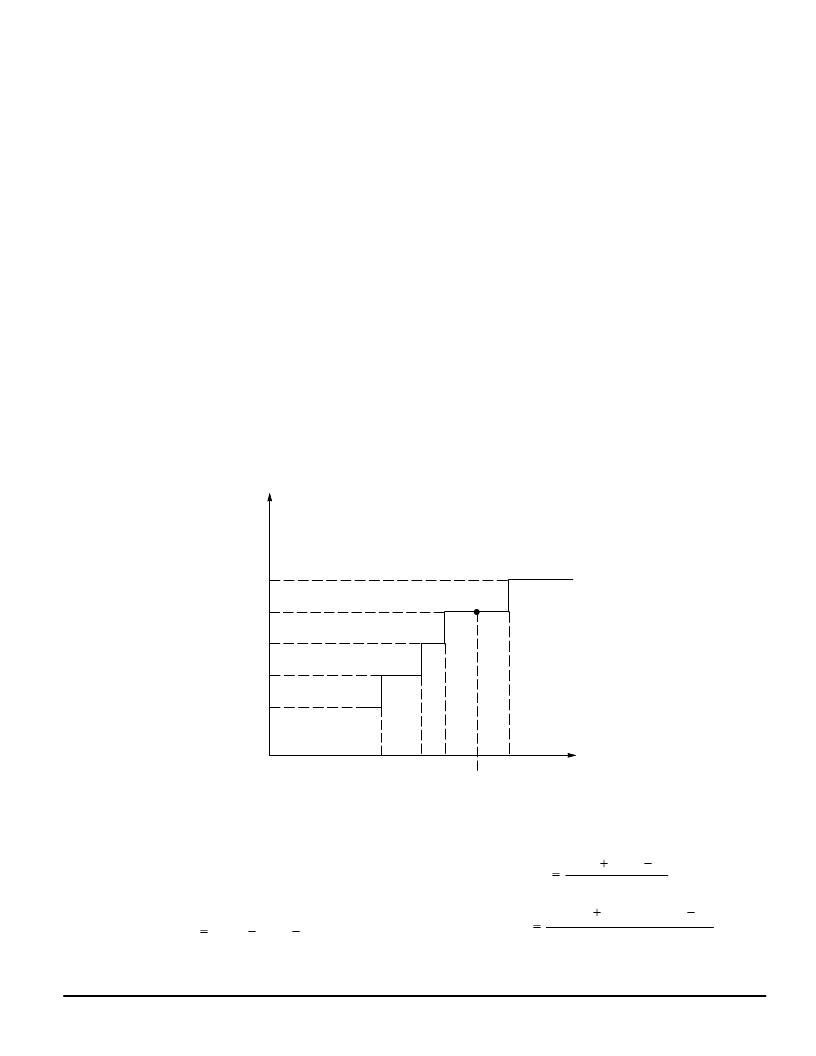
DEFINITIONS
n+4
VM (n+3)
n+3
n+2
n+1
n
VT (n) VT (n+1) VT (n+2)
VT (n+3)
Vin
OUTPUT
CODE
Figure 9.
Transition Voltage:
Voltage at which transition from step
n to step n+1 occurs = VT(n).
Step Size:
Difference between two consecutive transition
voltages.
SS(n)
VT(n)
VT(n
1)
Mid–Point Voltage:
VM(n)
VT(n)
VT(n
2
1)
VM(max code)
VDD(R)
VT(max code
2
1)
相關(guān)PDF資料 |
PDF描述 |
|---|---|
| MC44251FU | Triple 8-Bit Video ADC Three-State Outputs |
| MC44302ADW | ADVANCED MULTI-STANDARD VIDEO/SOUND IF |
| MC44302AP | ADVANCED MULTI-STANDARD VIDEO/SOUND IF |
| MC44353DTB | MULTI.STANDARD AND PAL/NTSC MODULATOR ICs |
| MC44353 | MULTI.STANDARD AND PAL/NTSC MODULATOR ICs |
相關(guān)代理商/技術(shù)參數(shù) |
參數(shù)描述 |
|---|---|
| MC44251FU | 制造商:MOTOROLA 制造商全稱:Motorola, Inc 功能描述:Triple 8-Bit Video ADC Three-State Outputs |
| MC4430 | 制造商:SHENZHENFREESCALE 制造商全稱:ShenZhen FreesCale Electronics. Co., Ltd 功能描述:N-Channel 30-V (D-S) MOSFET Fast switching speed |
| MC44302ADW | 制造商:MOTOROLA 制造商全稱:Motorola, Inc 功能描述:ADVANCED MULTI-STANDARD VIDEO/SOUND IF |
| MC44302AP | 制造商:MOTOROLA 制造商全稱:Motorola, Inc 功能描述:ADVANCED MULTI-STANDARD VIDEO/SOUND IF |
| MC4433 | 制造商:SHENZHENFREESCALE 制造商全稱:ShenZhen FreesCale Electronics. Co., Ltd 功能描述:P-Channel 30-V (D-S) MOSFET Fast switching speed |
發(fā)布緊急采購,3分鐘左右您將得到回復(fù)。