- 您現在的位置:買賣IC網 > PDF目錄371038 > MC54HC354J (MOTOROLA INC) 8-Input Data Selector/Multiplexer With Data and Address Latches and 3-State Outputs PDF資料下載
參數資料
| 型號: | MC54HC354J |
| 廠商: | MOTOROLA INC |
| 元件分類: | 通用總線功能 |
| 英文描述: | 8-Input Data Selector/Multiplexer With Data and Address Latches and 3-State Outputs |
| 中文描述: | HC/UH SERIES, 8 LINE TO 1 LINE MULTIPLEXER, COMPLEMENTARY OUTPUT, CDIP20 |
| 封裝: | CERAMIC, DIP-20 |
| 文件頁數: | 4/9頁 |
| 文件大小: | 206K |
| 代理商: | MC54HC354J |
MC54/74HC354
MOTOROLA
High–Speed CMOS Logic Data
DL129 — Rev 6
4
PIN DESCRIPTIONS
D0–D7 (Pins 8–1) DATA INPUTS
These eight data bits are stored in a transparent latch when
the Data–Latch Enable pin is active (high). Once enabled,
changing inputs will not change the contents of the latch.
A0, A1, A2 (Pins 14,13,12) ADDRESS INPUTS
Selects which data bit stored in the Data Latch is routed to
the outputs Y and Y.
DATA–LATCH ENABLE (Pin 9)
The latch is transparent to D0–D7 when enable is inactive
(low). The Data–Latch contents are unaffected when enable
is held active (high).
ADDRESS–LATCH ENABLE (Pin 11)
The latch is transparent to A0, A1 and A2 when enable is
inactive (low). The Address–Latch contents are unaffected
when enable is held active (high).
OE1, OE2, OE3 (Pins 15,16,17) OUTPUT ENABLES
Any of the output enable pins inactive (OE1=High or
OE2=High or OE3=Low) causes the outputs (Y and Y) to be
in high–impedance states.
Y, Y (Pins 19,18)
These 3–state outputs (when not 3–stated) represent the
data bit in the Data Latch selected by the Address Latch.
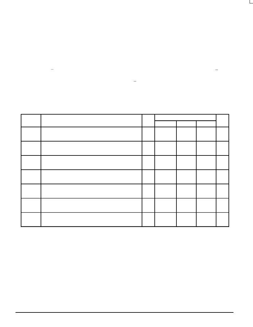
TIMING REQUIREMENTS
(Input tr = tf = 6 ns)
V
Guaranteed Limit
Symbol
Parameter
VCC
–55 to 25
°
C
≤
85
°
C
≤
125
°
C
Unit
tsu
Minimum Setup Time, D0–D7 to Data–Latch Enable
(Figure 5)
2.0
4.5
6.0
50
10
9
65
13
11
75
15
13
ns
tsu
Minimum Setup Time, A0–A2 to Address–Latch Enable
(Figure 5)
2.0
4.5
6.0
50
10
9
65
13
11
75
15
13
ns
th
Minimum Hold Time, Data–Latch Enable to D0–D7
(Figure 5)
2.0
4.5
6.0
5
5
5
5
5
5
5
5
5
ns
th
Minimum Hold Time, Address–Latch Enable to A0–A2
(Figure 5)
2.0
4.5
6.0
5
5
5
5
5
5
5
5
5
ns
tw
Minimum Pulse Width, Data–Latch Enable
(Figure 3)
2.0
4.5
6.0
80
16
14
100
20
17
120
24
20
ns
tw
Minimum Pulse Width, Address–Latch Enable
(Figure 3)
2.0
4.5
6.0
80
16
14
100
20
17
120
24
20
ns
tr, tf
Maximum Input Rise and Fall Times
(Figure 1)
2.0
4.5
6.0
1000
500
400
1000
500
400
1000
500
400
ns
NOTE:Information on typical parametric values can be found in Chapter 2 of the Motorola High–Speed CMOS Data Book (DL129/D).
相關PDF資料 |
PDF描述 |
|---|---|
| MC74HC354DW | 8-Input Data Selector/Multiplexer With Data and Address Latches and 3-State Outputs |
| MC74HC354 | 8-Input Data Selector/Multiplexer With Data and Address Latches and 3-State Outputs |
| MC74HC354N | 8-Input Data Selector/Multiplexer With Data and Address Latches and 3-State Outputs |
| MC54HC374AJ | Octal 3-State Noninverting D Flip-Flop |
| MC54HC374 | Octal 3-State Noninverting D Flip-Flop |
相關代理商/技術參數 |
參數描述 |
|---|---|
| MC54HC365 | 制造商:MOTOROLA 制造商全稱:Motorola, Inc 功能描述:Hex 3-State Noninverting Buffer with Common Enables |
| MC54HC365J | 制造商:MOTOROLA 制造商全稱:Motorola, Inc 功能描述:Hex 3-State Noninverting Buffer with Common Enables |
| MC54HC366 | 制造商:FREESCALE 制造商全稱:Freescale Semiconductor, Inc 功能描述:Hex 3-State Inverting Buffer with Common Enables |
| MC54HC366J | 制造商:MOTOROLA 制造商全稱:Motorola, Inc 功能描述:Hex 3-State Inverting Buffer with Common Enables |
| MC54HC367 | 制造商:MOTOROLA 制造商全稱:Motorola, Inc 功能描述:Hex 3-State Noninverting Buffer with Separate 2-Bit and 4-Bit Sections |
發布緊急采購,3分鐘左右您將得到回復。