- 您現在的位置:買賣IC網 > PDF目錄371042 > MC68160C (Motorola, Inc.) ENHANCED ETHERNET INTERFACE TRANSCEIVER PDF資料下載
參數資料
| 型號: | MC68160C |
| 廠商: | Motorola, Inc. |
| 英文描述: | ENHANCED ETHERNET INTERFACE TRANSCEIVER |
| 中文描述: | 增強型以太網接口的收發器 |
| 文件頁數: | 24/30頁 |
| 文件大小: | 372K |
| 代理商: | MC68160C |
第1頁第2頁第3頁第4頁第5頁第6頁第7頁第8頁第9頁第10頁第11頁第12頁第13頁第14頁第15頁第16頁第17頁第18頁第19頁第20頁第21頁第22頁第23頁當前第24頁第25頁第26頁第27頁第28頁第29頁第30頁
MC68160 MC68160B MC68160C
24
MOTOROLA ANALOG IC DEVICE DATA
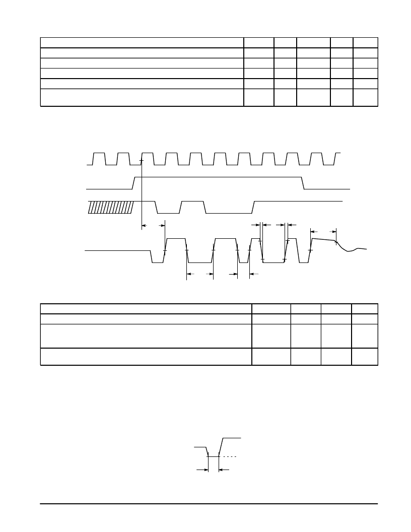
AUI TRANSMIT SWITCHING
Characteristic
Symbol
Min
Typ
Max
Unit
TCLK to ATX Pair Steady State Propagation Delay
t240
t241
t242
t243
t244
–
–
100
ns
Output Differential Rise and Fall Times (Measured directly at device pins)
1.0
–
5.0
ns
ATX Bit Cell Duration center–to–center (Measured directly at device pins)
–
99.5–100.5
–
ns
ATX Half–Bit Cell Duration center–to–boundary (Measured directly at device pins)
–
49.5–50.5
–
ns
ATX Pair Held at Positive Differential at start of Idle (Measured through
transformer)
200
–
–
ns
NOTE:
Load on specified output is a shunt 27
μ
H inductor and 83
resistor.
Figure 38. ATX Transmit Timings
1
0
1
TCLK
TENA
TX
ATX+/–
Differential
(Logic Levels)
0
0
1
1
1
1
1
1
0
0
0
t240
0V
t242
t243
t241
t241
t244
90%
10%
90%
10%
0V
1.5V
70%
AUI RECEIVE SWITCHING
Characteristic
Symbol
Min
Max
Unit
ARX/ACX Differential Input Voltage Range
–
±
318
±
1315
mV
ARX/ACX Differential Input Pulse Width to:
Initiate Data Reception
Inhibit Data Reception
t261
t262
30
–
–
18
ns
RENA Assertion Delay
RENA Deassertion Delay
t266
t267
–
–
100
450
ns
Squelching Characteristics
The receive data pairs and the collision pairs should have the following squelch characteristics:
1. The squelch circuits are on at idle (with input voltage at approximately 0 V differential).
2. If an input is in squelch, pulse is rejected if the peak differential voltage is more positive than –175 mV, regardless of pulse width.
3. A pulse is considered valid if its peak differential voltage is more negative than –300 mV and its width, measured at –285 mV, is > 25 ns.
4. The squelch circuits are disabled by the first valid negative differential pulse on either the AUI receive data or collision pair.
5. If a positive differential pulse occurs on either the AUI receive data or collision pair > 175 ns, end of frame is assumed and squelch circuitry is turned on.
t261/ t262
–175mV
+175mV
ARX+/–
ACX+/–
Differential
Input Voltage
Figure 39. ARX/ACX Timing
相關PDF資料 |
PDF描述 |
|---|---|
| MC68160CFB | 3.0V 100ppm/Degrees C, 50uA in SOT23-3 Series (Bandgap) Voltage Reference 3-SOT-23 -40 to 125 |
| MC68160FB | ENHANCED ETHERNET INTERFACE TRANSCEIVER |
| MC68175 | FLEXchip Decoder(FLEXchip譯碼器) |
| MC68176 | 2-bit A/D Converter(2位A/D轉換器) |
| MC68177 | FLEXchip Decoder(FLEXchip譯碼器) |
相關代理商/技術參數 |
參數描述 |
|---|---|
| MC68160CFB | 制造商:MOTOROLA 制造商全稱:Motorola, Inc 功能描述:ENHANCED ETHERNET INTERFACE TRANSCEIVER |
| MC68160FB | 制造商:Freescale Semiconductor 功能描述: 制造商:Motorola Inc 功能描述: 制造商: 功能描述: 制造商:undefined 功能描述: |
| MC68181 | 制造商:FREESCALE 制造商全稱:Freescale Semiconductor, Inc 功能描述:Advance Information ROAMING FLEX chip SIGNAL PROCESSOR |
| MC68184 | 制造商:MOTOROLA 制造商全稱:Motorola, Inc 功能描述:Broadband Interface Controller |
| MC68185 | 制造商:MOTOROLA 制造商全稱:Motorola, Inc 功能描述:MC68185 Twisted-Pair Modem(TPM) |
發布緊急采購,3分鐘左右您將得到回復。