- 您現在的位置:買賣IC網 > PDF目錄371059 > MC74AC823N (MOTOROLA INC) 9-BIT REGISTER WITH 3-STATE OUTPUTS PDF資料下載
參數資料
| 型號: | MC74AC823N |
| 廠商: | MOTOROLA INC |
| 元件分類: | 通用總線功能 |
| 英文描述: | 9-BIT REGISTER WITH 3-STATE OUTPUTS |
| 中文描述: | AC SERIES, 9-BIT REGISTERED TRANSCEIVER, TRUE OUTPUT, PDIP24 |
| 封裝: | PLASTIC, DIP-24 |
| 文件頁數: | 1/8頁 |
| 文件大小: | 219K |
| 代理商: | MC74AC823N |
5-1
FACT DATA
Product Preview
" "
"!
The MC74AC/ACT823 consists of nine D-type edge-triggered flip-flops. This
device has 3-state outputs for bus systems, organized in a broadside pinning. In
addition to the clock and output enabled pins, the buffered clock (CP) and buffered
Output Enable (OE) are common to all flip-flips. The flip-flops will store the state of
their individual D inputs that meet the setup and hold time requirements on the
LOW-to-HIGH CP transition. With OE LOW, the contents of the flip-flops are available
at the outputs. When OE is HIGH, the outputs go to the high impedance state.
Operation of the OE input does not affect the state of the flip-flops. The
MC74AC/ACT823 has Clear (CLR) and Clock Enable (EN) pins. These devices are
ideal for parity bus interfacing in high performance systems.
When CLR is LOW, and OE is LOW, the outputs are LOW. When CLR is HIGH,
data can be entered into the flip-flops. When EN is LOW, data on the inputs is
transferred to the outputs on the LOW-to-HIGH clock transition. When EN is HIGH,
the outputs do not change state, regardless of the data or clock input transitions.
3-State Outputs for Bus Interfacing
Broad Side Pin Configuration
ACT has TTL – Compatible Inputs
High Speed Parallel Positive Edge-Triggered D-Type Flip-Flops
High Performance Bus Interface Buffering for Busses Carrying Parity
Outputs Source/Sink 24 mA
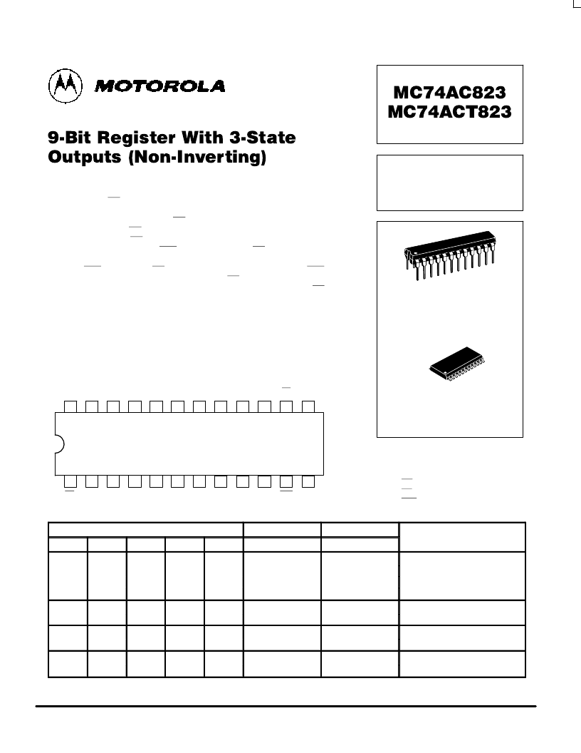
Pinout: 24-Lead Packages
(Top View)
23
24
22
21
20
19
18
VCC
17
O0
O1
O2
O3
O4
O5
O6
2
1
3
4
5
6
7
8
OE1
D0
D1
D2
D3
D4
D5
D6
16
9
O7
D7
15
10
O8
D8
14
11
EN
CLR
13
12
CP
GND
FUNCTION TABLE
Inputs
Internal
Outputs
Operating Mode
OE
CLR
EN
CP
Dn
Q
O
H
H
H
L
X
X
L
L
L
L
X
X
↑
↑
X
X
L
H
X
X
L
H
L
L
Z
Z
Z
L
High Z
High Z
Clear
Clear
H
L
H
H
H
H
X
X
↑
↑
↑
↑
X
X
NC
NC
Z
Hold
Hold
NC
H
H
H
H
L
L
L
H
L
H
Z
Z
Load
Load
L
L
H
H
L
L
L
H
L
H
L
H
Load
Load
H = HIGH Voltage Level; L = LOW Voltage Level; X = Immaterial; Z = High Impedance State;
↑
= LOW-to-High Transition; NC = No Change
This document contains information on a product under development. Motorola reserves the right to change or discontinue this product without notice.
9-BIT REGISTER WITH
3-STATE OUTPUTS
N SUFFIX
CASE 724-03
PLASTIC PACKAGE
1
24
PIN NAMES
Data Inputs
Data Outputs
Output Enable
Clock Enable
Clear
Clock Input
D0 – D8
O0 – O8
OE
EN
CLR
CP
DW SUFFIX
CASE 751E-04
SOIC PACKAGE
相關PDF資料 |
PDF描述 |
|---|---|
| MC74ACT823N | 9-BIT REGISTER WITH 3-STATE OUTPUTS |
| MC74ACT86 | QUAD 2-INPUT EXCLUSIVE-OR GATE |
| MC74ACT86D | QUAD 2-INPUT EXCLUSIVE-OR GATE |
| MC74ACT86DG | QUAD 2-INPUT EXCLUSIVE-OR GATE |
| MC74ACT86DTR2 | QUAD 2-INPUT EXCLUSIVE-OR GATE |
相關代理商/技術參數 |
參數描述 |
|---|---|
| MC74AC86 | 制造商:ONSEMI 制造商全稱:ON Semiconductor 功能描述:Quad 2−Input Exclusive−OR Gate |
| MC74AC86_06 | 制造商:ONSEMI 制造商全稱:ON Semiconductor 功能描述:Quad 2−Input Exclusive−OR Gate |
| MC74AC86D | 功能描述:邏輯門 2-6V Quad 2-Input RoHS:否 制造商:Texas Instruments 產品:OR 邏輯系列:LVC 柵極數量:2 線路數量(輸入/輸出):2 / 1 高電平輸出電流:- 16 mA 低電平輸出電流:16 mA 傳播延遲時間:3.8 ns 電源電壓-最大:5.5 V 電源電壓-最小:1.65 V 最大工作溫度:+ 125 C 安裝風格:SMD/SMT 封裝 / 箱體:DCU-8 封裝:Reel |
| MC74AC86DG | 功能描述:邏輯門 2-6V Quad 2-Input XOR RoHS:否 制造商:Texas Instruments 產品:OR 邏輯系列:LVC 柵極數量:2 線路數量(輸入/輸出):2 / 1 高電平輸出電流:- 16 mA 低電平輸出電流:16 mA 傳播延遲時間:3.8 ns 電源電壓-最大:5.5 V 電源電壓-最小:1.65 V 最大工作溫度:+ 125 C 安裝風格:SMD/SMT 封裝 / 箱體:DCU-8 封裝:Reel |
| MC74AC86DR2 | 功能描述:邏輯門 2-6V Quad 2-Input RoHS:否 制造商:Texas Instruments 產品:OR 邏輯系列:LVC 柵極數量:2 線路數量(輸入/輸出):2 / 1 高電平輸出電流:- 16 mA 低電平輸出電流:16 mA 傳播延遲時間:3.8 ns 電源電壓-最大:5.5 V 電源電壓-最小:1.65 V 最大工作溫度:+ 125 C 安裝風格:SMD/SMT 封裝 / 箱體:DCU-8 封裝:Reel |
發布緊急采購,3分鐘左右您將得到回復。