- 您現在的位置:買賣IC網 > PDF目錄371062 > MC74HC03 (Motorola, Inc.) Quad 2-Input NAND Gate With Open-Drain Outputs PDF資料下載
參數資料
| 型號: | MC74HC03 |
| 廠商: | Motorola, Inc. |
| 英文描述: | Quad 2-Input NAND Gate With Open-Drain Outputs |
| 中文描述: | 四2輸入與非門為開漏輸出 |
| 文件頁數: | 2/7頁 |
| 文件大小: | 175K |
| 代理商: | MC74HC03 |
MOTOROLA
High–Speed CMOS Logic Data
DL129 — Rev 6
2
SOIC Package
TSSOP Package
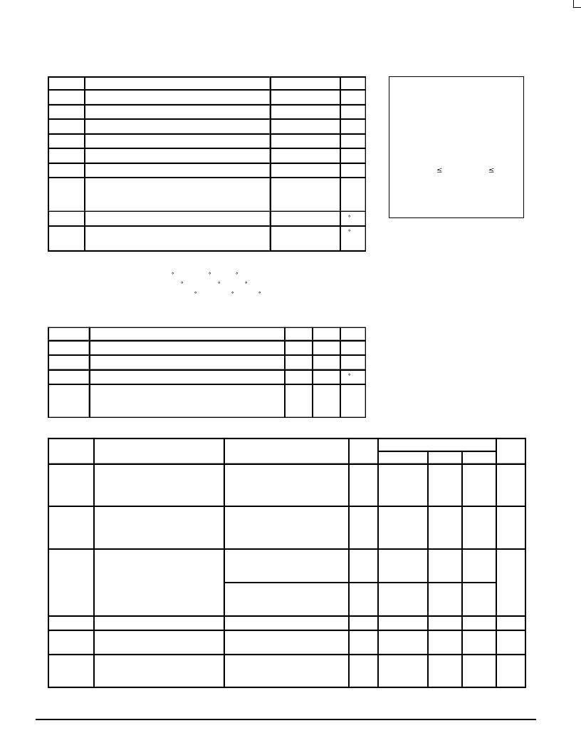
Tstg
TL
Storage Temperature
500
450
– 65 to + 150
C
Lead Temperature, 1 mm from Case for 10 Seconds
C
Functional operation should be restricted to the Recommended Operating Conditions.
Derating — Plastic DIP: – 10 mW/ C from 65 to 125 C
SOIC Package: – 7 mW/ C from 65 to 125 C
TSSOP Package: – 6.1 mW/ C from 65 to 125 C
0
400
VCC = 6.0 V
V
Guaranteed Limit
–55 to 25
°
C
Symbol
Parameter
Condition
VCC
≤
85
°
C
≤
125
°
C
Unit
VIH
Minimum High–Level Input Voltage
Vout = 0.1V or VCC –0.1V
|Iout|
≤
20
μ
A
2.0
3.0
4.5
6.0
1.50
2.10
3.15
4.20
1.50
2.10
3.15
4.20
1.50
2.10
3.15
4.20
V
VIL
Maximum Low–Level Input Voltage
Vout = 0.1V or VCC – 0.1V
|Iout|
≤
20
μ
A
2.0
3.0
4.5
6.0
0.50
0.90
1.35
1.80
0.50
0.90
1.35
1.80
0.50
0.90
1.35
1.80
V
VOL
Maximum Low–Level Output
Voltage
Vout = 0.1V or VCC – 0.1V
|Iout|
≤
20
μ
A
2.0
4.5
6.0
0.1
0.1
0.1
0.1
0.1
0.1
0.1
0.1
0.1
V
Vin = VIH or VIL
|Iout|
≤
2.4mA
|Iout|
≤
4.0mA
|Iout|
≤
5.2mA
3.0
4.5
6.0
0.26
0.26
0.26
0.33
0.33
0.33
0.40
0.40
0.40
Iin
ICC
Maximum Input Leakage Current
Vin = VCC or GND
Vin = VCC or GND
Iout = 0
μ
A
6.0
±
0.1
±
1.0
±
1.0
μ
A
Maximum Quiescent Supply
Current (per Package)
6.0
1.0
10
40
μ
A
IOZ
Maximum Three–State Leakage
Current
Output in High–Impedance State
Vin = VIL or VIH
Vout = VCC or GND
6.0
±
0.5
±
5.0
±
10
μ
A
NOTE: Information on typical parametric values can be found in Chapter 2 of the Motorola High–Speed CMOS Data Book (DL129/D).
This device contains protection
circuitry to guard against damage
due to high static voltages or electric
fields. However, precautions must
be taken to avoid applications of any
voltage higher than maximum rated
voltages to this high–impedance cir-
cuit. For proper operation, Vin and
Vout should be constrained to the
range GND (Vin or Vout)
Unused inputs must always be
tied to an appropriate logic voltage
level (e.g., either GND or VCC).
Unused outputs must be left open.
VCC.
相關PDF資料 |
PDF描述 |
|---|---|
| MC74HC03ADT | Quad 2-Input NAND Gate With Open-Drain Outputs |
| MC74HC03AN | Quad 2-Input NAND Gate With Open-Drain Outputs |
| MC74HC132 | Quad 2-Input NAND Gate with Schmitt-Trigger Inputs |
| MC74HC132 | Quad 2-Input NAND Gate with Schmitt-Trigger Inputs |
| MC74HC132AD | Quad 2-Input NAND Gate with Schmitt-Trigger Inputs |
相關代理商/技術參數 |
參數描述 |
|---|---|
| MC74HC03AD | 功能描述:邏輯門 2-6V Quad 2-Input RoHS:否 制造商:Texas Instruments 產品:OR 邏輯系列:LVC 柵極數量:2 線路數量(輸入/輸出):2 / 1 高電平輸出電流:- 16 mA 低電平輸出電流:16 mA 傳播延遲時間:3.8 ns 電源電壓-最大:5.5 V 電源電壓-最小:1.65 V 最大工作溫度:+ 125 C 安裝風格:SMD/SMT 封裝 / 箱體:DCU-8 封裝:Reel |
| MC74HC03ADG | 功能描述:邏輯門 2-6V Quad 2-Input NAND w/Open Drain RoHS:否 制造商:Texas Instruments 產品:OR 邏輯系列:LVC 柵極數量:2 線路數量(輸入/輸出):2 / 1 高電平輸出電流:- 16 mA 低電平輸出電流:16 mA 傳播延遲時間:3.8 ns 電源電壓-最大:5.5 V 電源電壓-最小:1.65 V 最大工作溫度:+ 125 C 安裝風格:SMD/SMT 封裝 / 箱體:DCU-8 封裝:Reel |
| MC74HC03ADR2 | 功能描述:邏輯門 2-6V Quad 2-Input RoHS:否 制造商:Texas Instruments 產品:OR 邏輯系列:LVC 柵極數量:2 線路數量(輸入/輸出):2 / 1 高電平輸出電流:- 16 mA 低電平輸出電流:16 mA 傳播延遲時間:3.8 ns 電源電壓-最大:5.5 V 電源電壓-最小:1.65 V 最大工作溫度:+ 125 C 安裝風格:SMD/SMT 封裝 / 箱體:DCU-8 封裝:Reel |
| MC74HC03ADR2G | 功能描述:邏輯門 2-6V Quad 2-Input NAND w/Open Drain RoHS:否 制造商:Texas Instruments 產品:OR 邏輯系列:LVC 柵極數量:2 線路數量(輸入/輸出):2 / 1 高電平輸出電流:- 16 mA 低電平輸出電流:16 mA 傳播延遲時間:3.8 ns 電源電壓-最大:5.5 V 電源電壓-最小:1.65 V 最大工作溫度:+ 125 C 安裝風格:SMD/SMT 封裝 / 箱體:DCU-8 封裝:Reel |
| MC74HC03ADT | 制造商:ON Semiconductor 功能描述:NAND Gate 4-Element 2-IN CMOS 14-Pin TSSOP Rail 制造商:Rochester Electronics LLC 功能描述:- Tape and Reel |
發布緊急采購,3分鐘左右您將得到回復。